Inside The IBM FlashSystem 900 All-Flash Array
The IBM FlashSystem family is the result of years of development and a $1 billion investment in flash technology, and it discards many of the commonly held design tenets of a typical all-flash array (AFA). The internal designs of AFAs are often closely guarded trade secrets. OEMs tend to focus on marketing data services but remain silent on the details of the architectural design.
IBM recently took us through the internal components of its FlashSystem 900, which serves as a standalone appliance that delivers up to 1 million/600,000 random read/write IOPS and 10.5/4.5 GBps of sequential read/write throughput. The FlashSystem 900 also serves as a building block for the IBM FlashSystem V9000 and A9000 AFAs, so our examination gives us a close-up look at the entire IBM FlashSystem product stack and allows us to investigate the difference between a system with commodity components and a custom design.
The Evolution Of All-Flash Arrays
Flash-based appliances evolved over several years, but they began with the use of commodity enterprise SSDs (such as standard 2.5" SAS or SATA SSDs) incorporated into existing storage appliances designed for HDDs. The speed of flash removes many of the performance bottlenecks associated with HDDs, but SSDs simply move the bottleneck to another component inside of the array (RAID controller or network interface) when employed as a drop-in HDD replacement.
The pioneers of the AFA movement began to develop SSD-optimized appliances with faster internal components and optimized data paths as the needs of the datacenter progressed, but each company embarked down its own developmental path. The majority of AFA vendors still employ 2.5" SSDs. The newest AFAs based on 2.5" SSDs offer plenty of performance and endurance, but internal SSD functions are locked behind the SSD vendors' firmware.
Other vendors, such as IBM, XtremIO (EMC) and Violin, developed their own AFAs with custom flash modules. These new designs provide the vendor with an unprecedented amount of control of the NAND itself, which unlocks additional storage density, performance, endurance and cost efficiency.
IBM FlashSystem 900
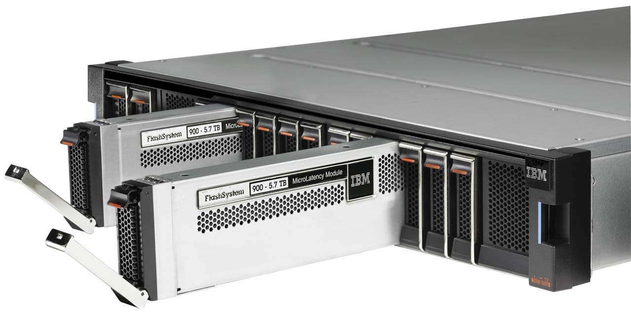
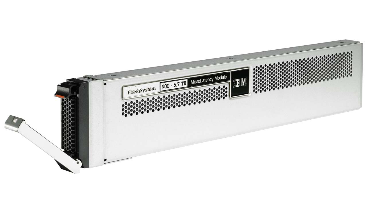
The 2U FlashSystem 900 chassis employs 12 hot-swappable MicroLatency Modules, as seen in the image below. The system also has two large Lithium-ion battery packs (far left) that provide enough power to flush all data in transit to the underlying flash in the event of an unsafe power loss. The batteries provide enough power to complete this process back-to-back, if needed.
Each MicroLatency Module can contain 1.2 TB, 2.9 TB or 5.7 TB of flash, and the system stripes data across the modules in a RAID 5 configuration to ensure there is no data loss in the event of a failure. IBM also employs its own variable-stripe RAID at the flash level to create a two-dimensional parity scheme.
Get Tom's Hardware's best news and in-depth reviews, straight to your inbox.
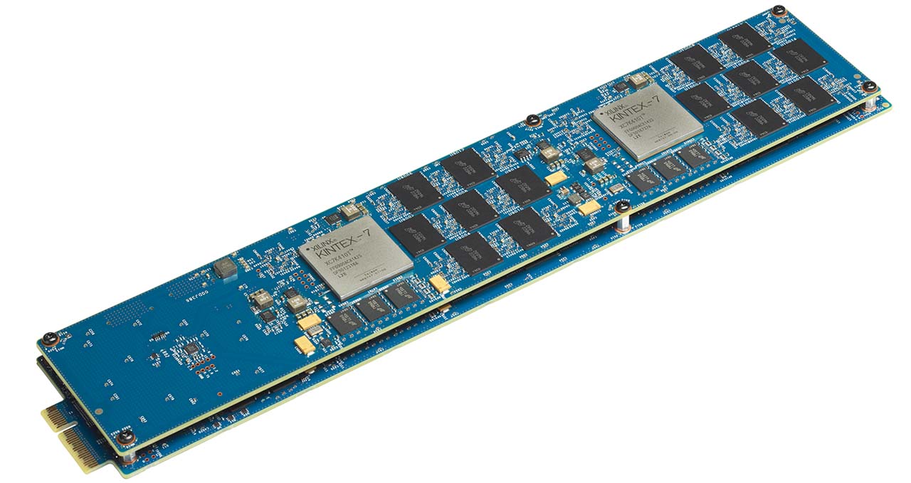
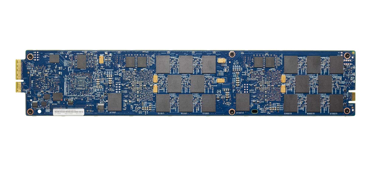
Each MicroLatency Module has a dual-PCB design with Xilinx Kintex-7 FPGAs. Each PCB can house up to four FPGAs, but the number of FPGAs present on each card varies based upon module density. For instance, a 1.2 TB module will employ only one FPGA on a single PCB. The use of a multiple-FPGA architecture allows IBM to scale steady-state performance and capacity in a linear fashion.
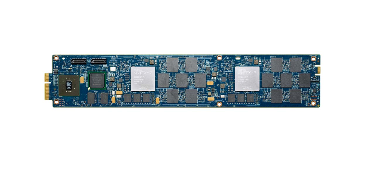
A closer look at the bottom PCB reveals the two PCIe 3.0 x2 connections on the left. These connectors slot into the host and communicate using an IBM-proprietary serial protocol that delivers many of the same benefits of NVMe, such as reduced CPU overhead and latency, in tandem with increased performance. The proprietary protocol utilizes a hardware-accelerated data path with cut-through routing to eliminate latency-inducing processes, such as interrupts.
Each FPGA has its own DRAM emplacements for LBA management tasks, and IBM also employs the DRAM for caching user data. Most enterprise SSDs do not cache user data in the DRAM, but the system-level approach to power loss protection (via batteries) affords IBM several design advantages. The individual SSDs do not require dedicated capacitors, such as those found on commodity SSDs, which allows the company to pack more flash into the design. The capacitor-less design also reduces potential points of failure and firmware complexity.
We did note a few capacitors spread among the flash packages, but these are used to combat voltage droop when the system writes to several NAND packages simultaneously.
IBM forged a strategic partnership with Micron to use FortisFlash NAND, which is customizable and exposes additional programming hooks to the system. This allows IBM to dynamically alter the base programming of each block over the course of the NAND's life based upon age and health. Micron has indicated that, with the correct tuning, MLC FortisFlash NAND can offer up to 10,000 write-erase cycles (more than triple the standard 3,000-cycle rating).
There are many different flavors of ECC, such as BCH and LDPC, and each has its own advantages and disadvantages. AFA vendors that employ commodity 2.5" SSDs are limited to the ECC that comes from the SSD vendor, but a custom design provides the flexibility to employ custom ECC algorithms.
IBM developed a proprietary “read once” ECC algorithm. This implementation straddles the line between BCH, which is capacity-intensive and has limited error correction capability, and LDPC, which can incur excessive write amplification during the error-correction process (thus reducing endurance). IBM feels the custom "read once" error correction provides the best of both worlds.
IBM also employs heat segregation, which detects hot and cold data and then pools it to reduce wear. IBM dynamically detects the remaining endurance of each cell, so it can store less frequently-accessed "cold" data on older NAND cells, thus preserving the endurance and mitigating other endurance-reducing tendencies, such as read disturbs. IBM claimed that heat segregation increases endurance by 49 percent, and the addition of selective wear leveling (based upon NAND health) increases endurance another 57 percent.
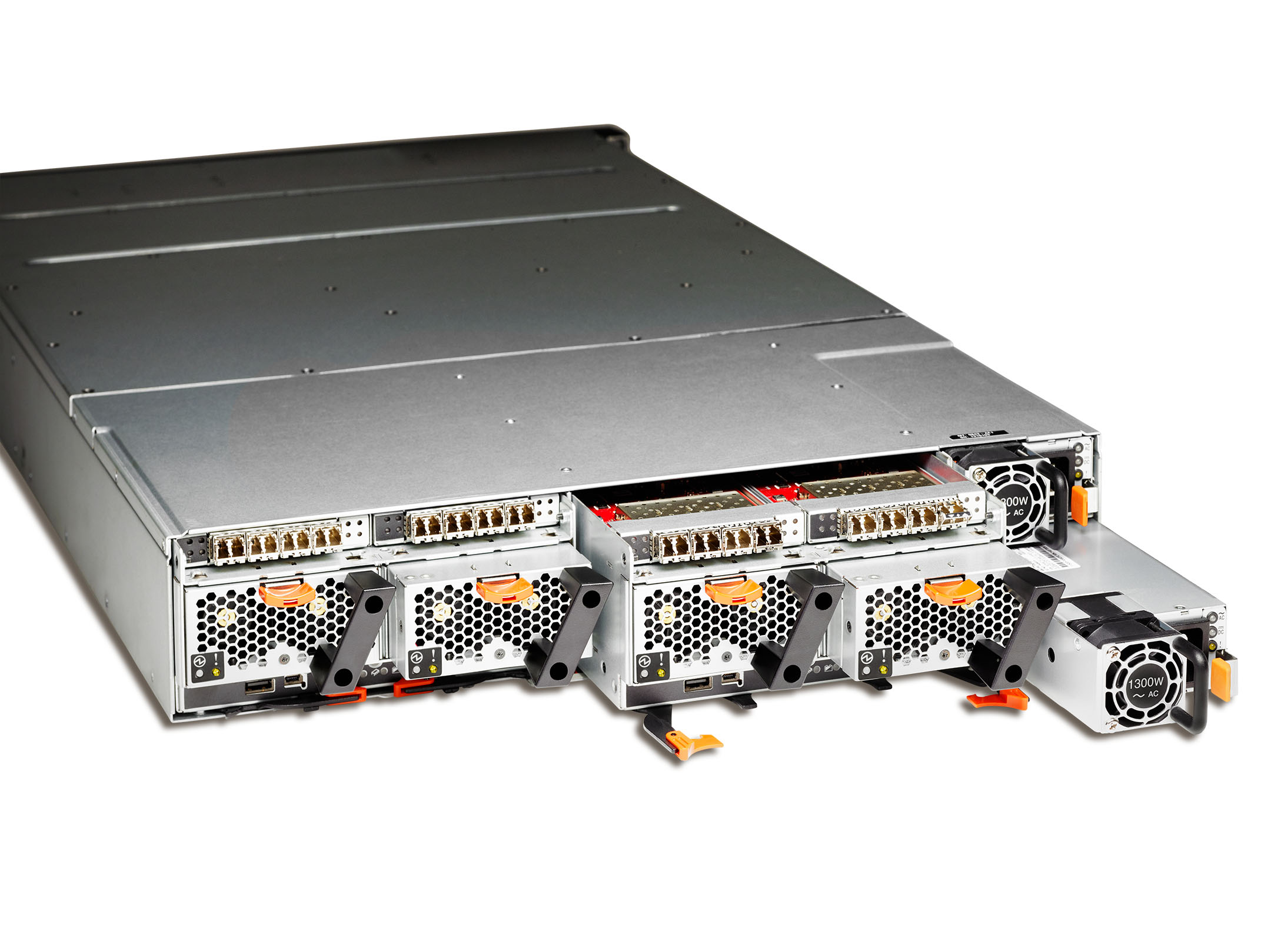
Each 2U chassis houses two hot-swappable redundant power supplies (right) behind the front-panel accessible batteries. The system features four hot-swappable fan modules that slot into two larger canister assemblies. Each of the two large canisters (left) hold a row of I/O ports (a range of Fibre Channel, iSCSI and FCoE options) along the top that reside on hot-swappable interface cards.
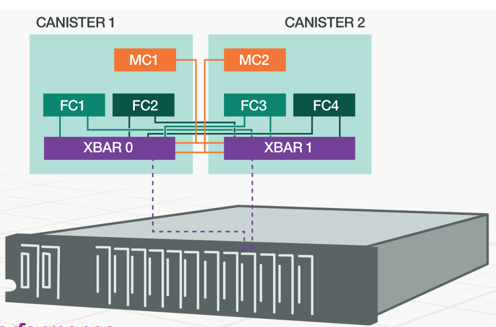
Each canister contains two Intel Xeon E5 v2 CPUs, 64 GB of RAM and a RAID controller (XBAR). The canisters are also hot-swappable to ensure that there is no downtime in the event of a compute or memory failure, and the design is optimized to ensure that there are never more than two "hops" from the I/O ports to the flash, which ensures consistent performance and latency.
The Broader Relevance
IBM purchased Texas Memory Systems in 2012 and made an additional $1 billion investment in flash technology development in 2013, which enabled the company to develop a customized all-flash array that offers advantages beyond some typical all-flash arrays. IBM claimed that the FlashSystem family offers up to 9.41 percent more endurance than competing solutions, and backs it with a seven-year guarantee.
IBM is able to add more density through a custom MicroLatency Module design that reaps the benefits of system-wide power loss protection, and it even employs its own custom hardware-driven serial interface that eliminates software-induced latency. IBM designed the architecture to provide incredibly granular advantages, such as custom ECC and adaptive NAND algorithms, which provide big benefits to its customers in terms of density, performance and cost.
IBM is not the only horse in the custom all-flash array race. EMC recently unveiled an entire line of flash-based appliances, some of which employ custom SSD designs, and the company is transitioning all of its storage systems to all-flash. Pure Storage also has a budding initiative with its FlashBlade appliance, but it is not generally available as of yet. Violin Memory also has a custom design, but its poor company performance and dismal prospects dissuade many from utilizing its solutions.
IBM is among the top AFA vendors in terms of capacity shipped, but not in revenue. IBM claimed the disparity is the end result of its custom design that offers more flash capacity for fewer dollars than its competitors.
It is clear that the future of flash-based technology will feature even more customized and optimized designs. This will likely lead to the demise of many of the systems (and companies) employing commodity SSDs--especially if the industry begins to adopt flash-aware software.
Paul Alcorn is a Contributing Editor for Tom's Hardware, covering Storage. Follow him on Twitter and Google+.
Follow us @tomshardware, on Facebook and on Google+.

Paul Alcorn is the Editor-in-Chief for Tom's Hardware US. He also writes news and reviews on CPUs, storage, and enterprise hardware.
