Hacktivists share a guide on making working electronics PCBs made from natural clay with prehistoric technique — ethical hardware tutorial explains how to find clay, stamp 3D printed circuits, paint traces, and fire tablets
The method shared is open source, avoids plastics and conflict minerals, and looks like fun.
There comes a time for many electronics enthusiasts and tinkerers when they wish they had a custom-made PCB for a project. If you enjoy a bit of crafting, the netizens over at Feminist Hacking might have a compelling solution for PCB-needy DIYers, using real clay to produce working PCBs, as shared in a blog post headed “MaKING Printed Circuit Boards with Wild Clay.”
The hacktivists behind this project didn’t just want a craft project as a source of artistic satisfaction. This is made clear in the intro to the blog, where they ponder the “open secret that the hardware in our smart devices contains not only plastics but also conflict minerals.” However, it didn’t take long to narrow down the options to come up with the idea of clay PCBs.
Porcelain “already plays an important role in electronic components such as capacitors, piezo, resistors, and so on,” note the hacktivists. But they didn’t want to buy commercial china clay or use expensive, unsustainable, resource-draining firing techniques.


'Prehistoric techniques of firing clay'
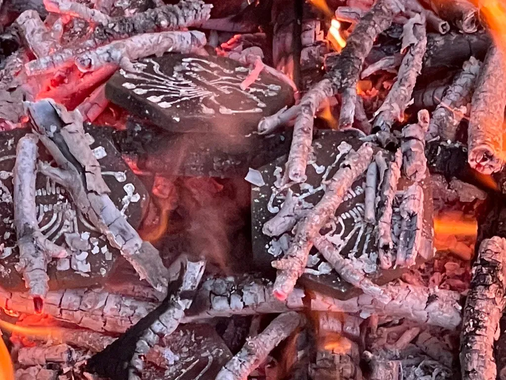
After some research, they learned from a pottery artisan that you can use “prehistoric techniques of firing clay in an open wood fire” to do the job. After spending two days with this craftsperson, the hacktivists learned to locally source clay, work it, and fire it to make these “natural clay PCB boards.”
The blog gives tips for collecting and mixing clay, ready for working into rounds, with all air and impurities minimized. That’s important for uniform, consistent, well-behaved clay PCBs.
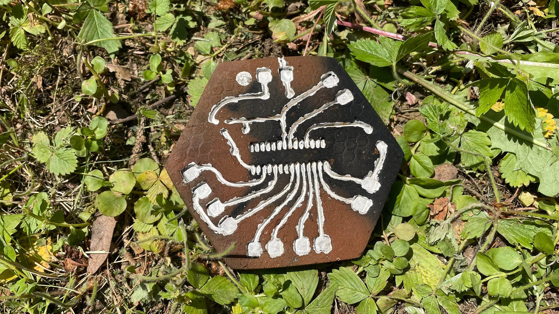
A hexagon shape was chosen as this cookie cutter “can be bought in most ceramic shops,” but only rough dimensions of approx 10x10cm (~4x4 inches) are required, not any particular shape. Originally, the hexagon was chosen to make the PCBs easy to connect, but that idea has been shelved as the fired tablet edges aren’t that precise.
Remember, we are working with less elastic and more fragile clay than you may get in a craft store. The hacktivists note it might be rough or split at the edges. As long as the inner cutter area removes this, it isn’t a problem.
Get Tom's Hardware's best news and in-depth reviews, straight to your inbox.
Stamp PCB traces with a 3D-printed template, and paint traces in silver
Pressing the 3D-printed stamp into the clay needs some experience. It is important to balance pressure to get the optimal impression depth of roughly 1.5mm without deforming the surrounding areas. The pressed hexagon PCB tablets are dried naturally for a day before metal traces are hand-painted in the impressions.
The hacktivists avoided using a conductive gold paint they initially found, as it wasn’t really suitable for solder bonding, and came from a supply chain that wasn’t verified. Silver was the answer, specifically “a silver paint, commercialized by a German company, that is made with waste silver powder collected by jewelry makers.” More paint was applied to areas where you may expect to solder connections, later.
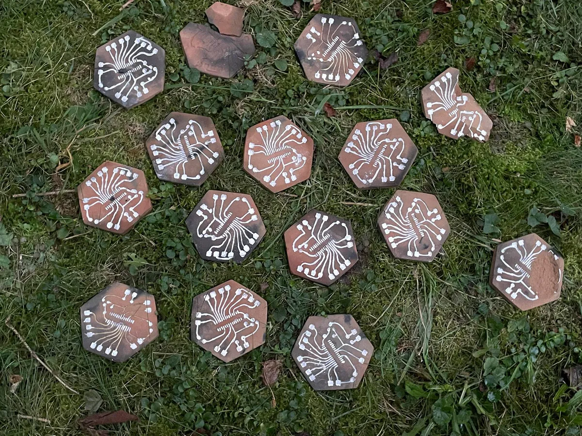
After the paint had dried, the clay PCBs were ready to fire. The blog wraps up with a detailed set of instructions regarding the prehistoric firing process. One aspect of the process that needed refinement from the hacktivists was the effects of clay shrinkage in the firing kiln. Clay can shrink 5% in firing, so there was a little trial and error in getting the stamp size and groove depth correct in finished PCBs.
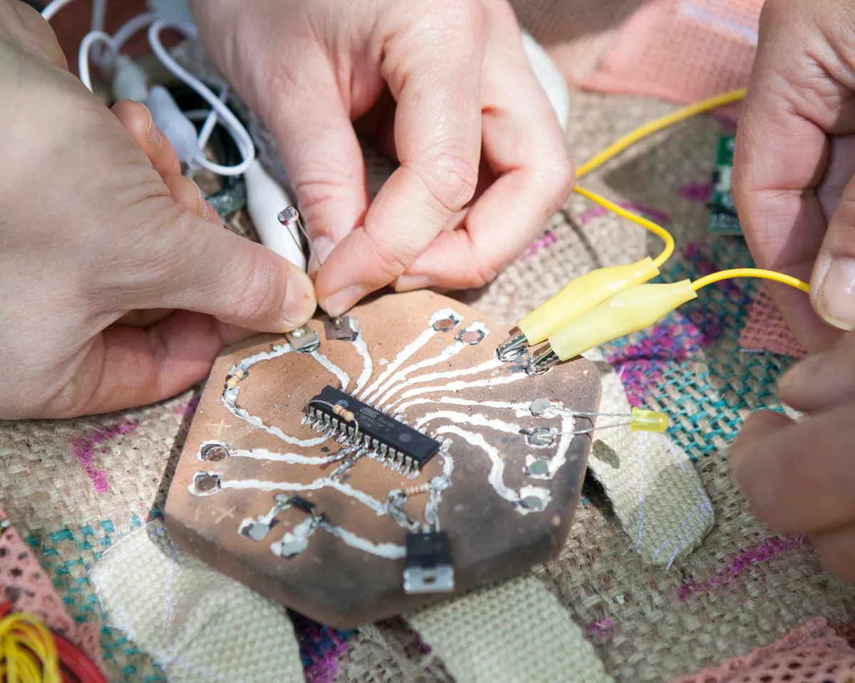
Finally, this project is “totally open sourced,” so feel free to copy and share the details in the hacktivist blog. There’s even a PDF available, should you require one. The team also has a GitHub page with programming code, soldering instructions, and 3D printing files available.
Follow Tom's Hardware on Google News, or add us as a preferred source, to get our latest news, analysis, & reviews in your feeds.

Mark Tyson is a news editor at Tom's Hardware. He enjoys covering the full breadth of PC tech; from business and semiconductor design to products approaching the edge of reason.
-
bit_user Just curious whether they actually called themselves "hacktivists", or whether that's a liberty taken by the author.Reply
"Hacking" doesn't necessarily have a negative connotation, but I think you can't just apply "hacktivist" to every scenario where you might call someone a "hacker", as it does tend to have a more destructive connotation. -
IntelUser2000 It's mildly interesting but it's not really usable. Once things need to be commercialized, you need it to be cheap, readily mass produced, and durable.Reply
Problems like conflict materials and waste is a human nature flaw issue, not something that'll ever solved by technology. Technology often amplifies the issue, never solves them. -
Just Dave Reply
It also doesn't seem especially disruptive. More of a fun builder project. I can't imagine they're deluded enough to think this is actually more ecologically viable at scale than current PCB technology, so it's not going to displace it.bit_user said:Just curious whether they actually called themselves "hacktivists", or whether that's a liberty taken by the author.
"Hacking" doesn't necessarily have a negative connotation, but I think you can't just apply "hacktivist" to every scenario where you might call someone a "hacker", as it does tend to have a more destructive connotation. -
Gururu Reply
Did you even read the source? The group is literally called Feminist Hacking.bit_user said:Just curious whether they actually called themselves "hacktivists", or whether that's a liberty taken by the author.
"Hacking" doesn't necessarily have a negative connotation, but I think you can't just apply "hacktivist" to every scenario where you might call someone a "hacker", as it does tend to have a more destructive connotation. -
IntelUser2000 Reply
They would need to increase the precision *greatly* to even support cheap electronics nowadays. I know, because I created 2-layer PCBs before for 1.8mm x 1mm IC with ball grid array successfully many times.Just Dave said:It also doesn't seem especially disruptive. More of a fun builder project. I can't imagine they're deluded enough to think this is actually more ecologically viable at scale than current PCB technology, so it's not going to displace it.
Try looking up a cheap USB-C adapter and see how complex the routing is for the microcontroller.
Actually for hobbyist we already have an "eco-friendly" alternative. I use a good laser printer that can put out thick toner and a proper thermal transfer paper with a laminator to transfer the toner. Then it's etched using Ferro Chloric acid.
But instead of insane waste of keeping and maintaining a huge vat or FeCL acid, I take a table spoon inside a ziploc bag and "massage" the board from the outside. The physical movement overcomes surface tension and is far more effective and needs only a teeny amount of FeCL to work, which later I put in a single sheet of half-sized paper towel and dries to nothing in a day. You get basically a towel that is smudged with completely dry Iron + Copper, because the tiny amount gets completely saturated with etched copper, unlike unimaginable waste with vat of FeCL.
I can make a dozen board and the bag and paper towel takes almost no space and is completely safe to store, with no used FeCL to throw away. Plus, a litre of FeCL would last basically forever with only a tablespoon used for a small board.
It's also far less damaging on the circuit and thus I get a better quality over putting in a vat. The fancy bubble machines are useless and are money wasters. 5 min of "massaging" does a far better job, no comparison and costing me literal cents plus zero harm to me or the environment. -
bit_user Reply
Yes, I did.Gururu said:Did you even read the source?
The mere fact of someone having a political ideology doesn't make them hacktivists. If they had a political ideology and did some vandalism (or worse), that would make them hactivists.Gururu said:The group is literally called Feminist Hacking.
This site has a history of trying to "punch up" article titles, to get more clicks. I try to point out when they cross the line over to something that's misleading (which isn't uncommon).
BTW, whether or not you agree with their ideology doesn't make it okay to mischaracterize someone. "Hacktivist" is a loaded term. I wouldn't call someone that, unless they either referred to themselves that way or clearly fit the most established definition. -
Gururu Reply
Ok I see what you are getting at and agree. I guess adding the suffix to it kind of denigrates it in some way by insinuating their motives are political.bit_user said:Yes, I did.
The mere fact of someone having a political ideology doesn't make them hacktivists. If they had a political ideology and did some vandalism (or worse), that would make them hactivists.
This site has a history of trying to "punch up" article titles, to get more clicks. I try to point out when they cross the line over to something that's misleading (which isn't uncommon).
BTW, whether or not you agree with their ideology doesn't make it okay to mischaracterize someone. "Hacktivist" is a loaded term. I wouldn't call someone that, unless they either referred to themselves that way or clearly fit the most established definition.