Evolution Of Intel Graphics: i740 To Iris Pro
Get Tom's Hardware's best news and in-depth reviews, straight to your inbox.
You are now subscribed
Your newsletter sign-up was successful
Intel Enters The GPU Race
In the world of graphics processing, AMD and Nvidia take center stage in terms of performance and the amount of attention we give them. Although these companies have gained renown for their technologies, neither of them are the largest GPU vendor. Intel holds that distinction. The company has tried to compete with AMD and Nvidia for the performance crown, at times even producing full graphics cards. But really, its strength is building graphics technology into its chipsets and processors. This effectively puts Intel's GPUs into a majority of today's computers. Because of the constraints placed on integrated solutions, though, the company's graphics engines are typically known for entry-level performance. Its most recent efforts are far more impressive, some of them going so far as to outpace entry-level discrete cards from AMD and Nvidia. Intel's HD Graphics may lag behind the others, but the fact is the days of the GMA 950 and its predecessors are over.
Intel's First Dedicated GPU: The i740 (1998)
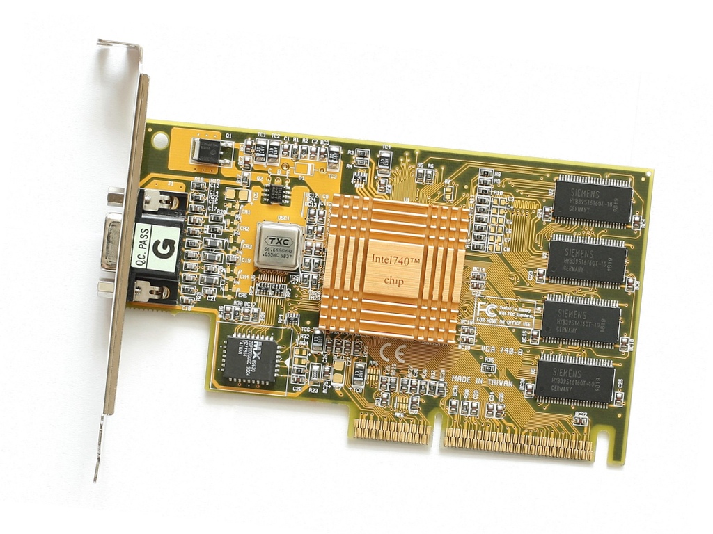
In 1998, Intel launched its first graphics card: the i740 code-named "Auburn." It was clocked at 220MHz and employed a relatively small amount of VRAM between 2 and 8MB. Comparable cards cards of the time typically included at least 8MB and ranged up to 32MB. It also supported DirectX 5.0 and OpenGL 1.1. In order to get around the shortage of on-board memory, Intel planned to take advantage of a feature built into the AGP interface that allowed the card to utilize system RAM. As such, the i740 uses the on-board memory only as a frame buffer, while storing all textures inside of the platform's memory. Without having to pay as much for pricey RAM, Intel sold its i740 at a relatively low cost. Unfortunately, the GPU encountered a number of difficulties. System RAM couldn't be accessed as quickly as on-board memory, which negatively impacted performance. It also reduced CPU performance, as the processor had less bandwidth and memory to work with. Early drivers further crippled the card's performance, and its picture quality was questionable because of a slow RAMDAC. The i740 ultimately proved to be a disaster. Intel attempted to improve the situation by compelling motherboard manufacturers to bundle the card with 440BX-based platforms, but this failed too.
i752 Graphics Chip And The 81x Series Chipsets (1999)
After the i740 disaster, Intel developed and briefly sold a second graphics card named the i752 "Portola", though in very limited quantities. Around the same time, Intel began using its graphics technology inside of chipsets like the i810 ("Whitney") and i815 ("Solano"). The GPU was incorporated into the northbridge, becoming the first integrated graphics processors sold by Intel. Their performance was dependent on two factors: RAM speed, which was often linked to the FSB, and in turn dependent on the processor, and the CPU itself. At the time, Intel used 66, 100 or 133MHz FSB configurations alongside asynchronous SDRAM, giving the system a maximum bandwidth of 533, 800 or 1066 MB/s, respectively. Although this throughput was shared with the processor, the iGPU never had access to the whole pipe. Motherboard manufacturers could optionally place 4MB of dedicated video memory onto their platforms, connected directly to the graphics processor via AGP x4 and providing an additional 1066 MB/s.
Article continues belowThe performance of these iGPUs was low. Further, the i810 chipset lacked an AGP interface due to the integrated graphics, thus limiting upgrades to slower PCI-based graphics cards. The i815 chipset allowed for an AGP port in addition to the iGPU, but installing a discrete card disabled the iGPU. As a result, these graphics solutions were aimed at low-end budget users.
Intel Extreme Graphics (2001)
In 2001, Intel began its Extreme Graphics family, which was closely related to the previous generation, including two pixel pipelines and limited MPEG-2 hardware acceleration. Software API support was nearly identical to the i815 chipsets, although OpenGL support was extended to version 1.3 of the API.
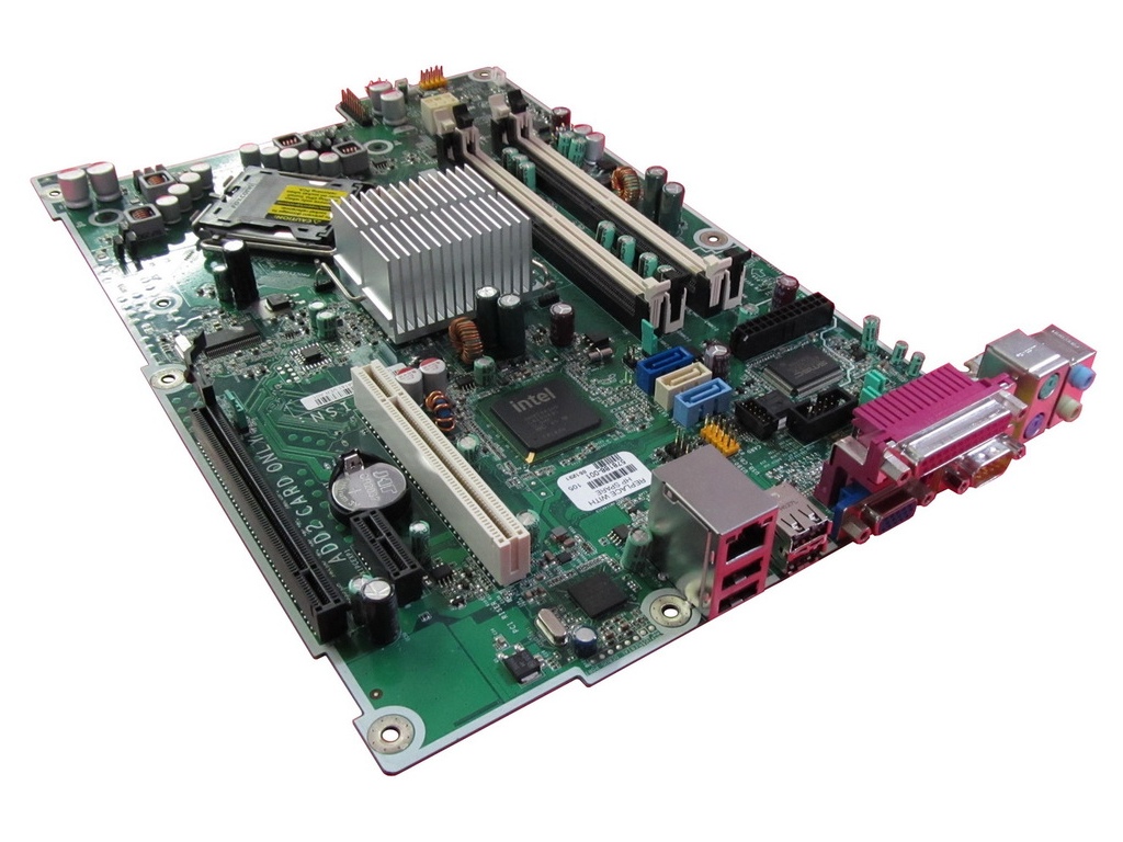
The performance of Intel's Extreme Graphics iGPUs was heavily dependent on the chipset, RAM and processor. The first implementation appeared inside of Intel's i830 chipset family (Almador), which was designed for Pentium III-M. These systems continued to use aging SDRAM memory, which limited them to a maximum of 1066 MB/s of bandwidth, similar to earlier GPUs. Clock rate dropped from the i815's 230MHz to 166MHz on the Almador chipsets to conserve power and reduce heat output.
The desktop implementation was released later in 2002 inside of the i845 Brookdale chipsets, designed for Pentium 4 processors. These systems also ran at a lower clock rate than the i815 chipsets (200MHz), though they could use SDRAM or DDR memory. Thanks to faster host processors, the i845 chipset iGPU paired with SDRAM performed better than the i815 models, despite the lower frequency. Implementations using DDR RAM pushed performance even higher. These integrated solutions weren't quick enough to beat Nvidia's GeForce 2 Ultra, a graphics card that was over a year old at the time. But they were sufficient for light gaming.
Get Tom's Hardware's best news and in-depth reviews, straight to your inbox.
Intel Extreme Graphics 2 (2003)
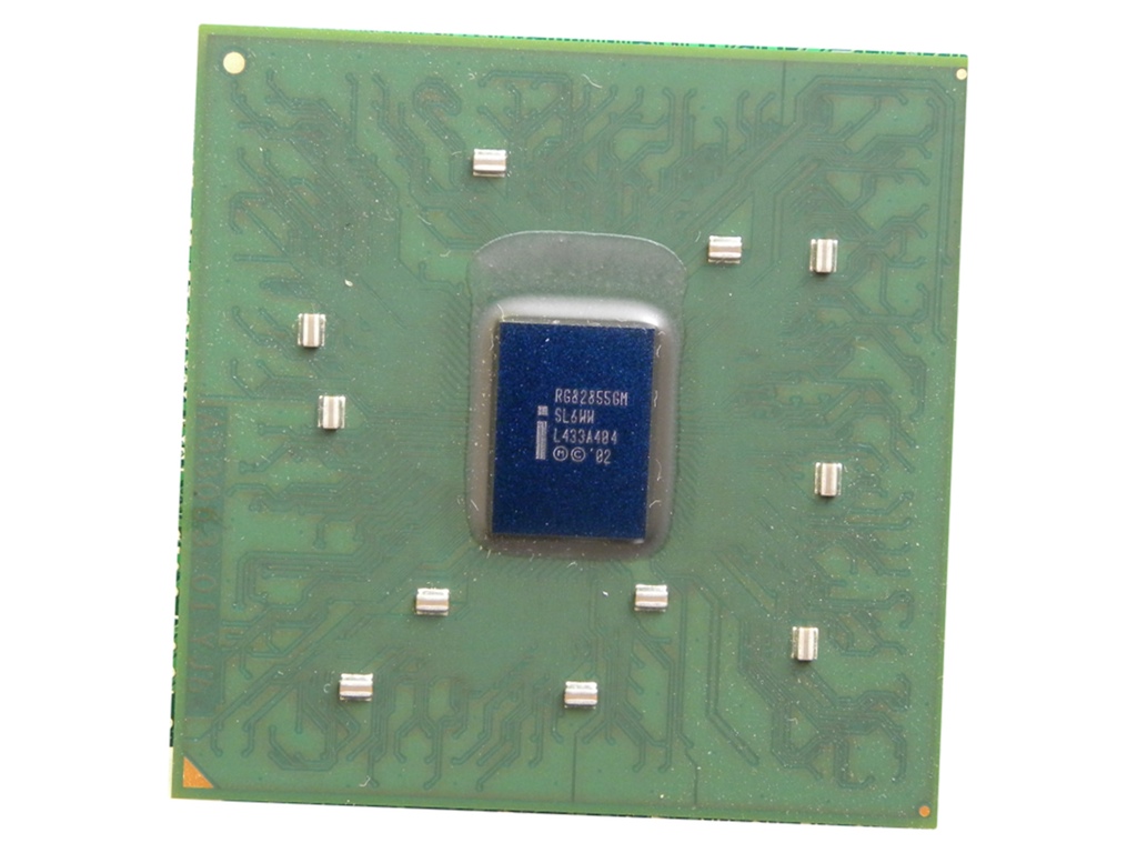
Intel reused the two-pixel-pipeline graphics chip one more time in its Extreme Graphics 2 family, released in 2003. The company again introduced two versions. A mobile implementation surfaced first, appearing in the i852 and i855 chipsets designed for the Pentium M. These versions of the chip operated anywhere between 133 and 266MHz, depending on the OEM's design choice. The second version was used inside of the i865 Springdale chipsets designed for the Pentium 4. These always operated at 266MHz and used faster DDR memory that could operate at up to 400MHz, giving them higher bandwidth than prior iGPUs.
Although performance increased considerably compared to the older Intel Extreme Graphics line, games had also advanced, becoming significantly more demanding. As a result, these graphics chips were only capable of playing older games at passable frame rates.
The GMA 900 (2004)
In 2004, Intel brought its Extreme Graphics line-up to an end, retiring the two-pixel-pipeline core that was used in all prior Intel GPUs. The Graphics Media Accelerator (or GMA) would be the name used by Intel to sell its graphics technology for the next several years. The first of these products, GMA 900, was integrated into the i915 chipset family (Grantsdale/Alviso). It featured support for DirectX 9.0 and contained four pixel pipelines, but lacked vertex shaders, instead relying on the CPU to do these calculations. The GPU could be clocked as high as 333MHz or as low as 133MHz for power-sensitive applications, and could use either DDR or DDR2 memory. Regardless of the configuration, performance was relatively low.
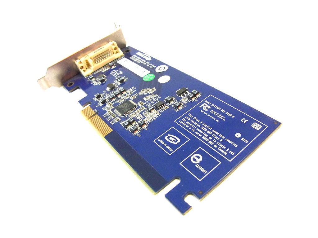
Some manufacturers produced special add-on cards for use in conjunction with the GMA 900 in order to add DVI connectivity.
GMA 950: Pentium 4 & Atom (2005)
The GMA 950 was integrated into Intel's i945 (Lakeport and Calistoga) chipsets, and enjoyed a relatively long life. These chipsets were capable of working with Pentium 4, Core Duo, Core 2 Duo and Atom processors. The architecture was nearly identical to the GMA 900, however, inheriting many of the same weaknesses, including a lack of vertex shaders. The core did receive some minor software compatibility improvements, extending DirectX support to 9.0c. This was an important update to the graphics chip, as it enabled Aero support on Windows Vista. Performance increased slightly thanks to a frequency bump (400MHz) and support for faster processors and RAM. Mobile versions of the GPU could be as clocked as low as 166MHz to conserve power and to satisfy thermal constraints.
The GMA 3000, 3100 & 3150 (2006)
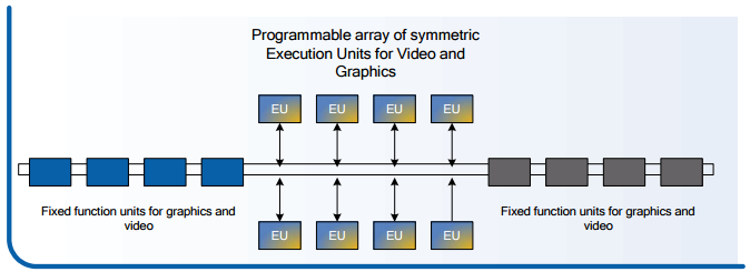
In 2006, Intel again changed its graphics nomenclature, starting with the GMA 3000. This was a considerable step up from the older GMA 950 in terms of performance and technology. The previous generation was limited to four fixed-function pixel pipelines without vertex shadings. Meanwhile, the new GMA 3000 included eight multi-purpose EUs that were capable of performing multiple tasks including vertex calculations and pixel processing. Intel pushed its clock rate to 667MHz as well, making its GMA 3000 considerably faster than the older GMA 950.
After introducing GMA 3000, Intel added two more graphics chips to the family: GMA 3100 and the GMA 3150. Although they appeared related to the 3000, both configurations were actually more similar to GMA 950. They only came with four pixel pipelines and relied on the CPU for vertex processing. Prior to this, Intel focused on one GPU at a time. The recycling of GMA 950 rebranded as GMA 3100 and 3150 allowed Intel to offer multiple configurations.
GMA X3000 (2006)
After the GMA 3000, Intel made another modification to its naming, creating a fourth generation of GPUs. The GMA X3000 was nearly identical to the GMA 3000, however, only incorporating minor changes. The most significant difference between them was that GMA 3000 could only use 256MB of system memory for graphics, while the GMA X3000 could use up to 384MB. Intel also extended GMA X3000's video codec support to include full MPEG-2 and limited VC-1 acceleration.
Around the same time, Intel introduced the GMA X3100 and the GMA X3500. These models were essentially the same as the GMA X3000 upgraded with Pixel Shader 4.0 functionality, allowing them to support newer APIs like DirectX 10. The GMA X3100 was clocked lower than the other versions, as it was targeted at mobile platforms.
The Last GMA (2008)
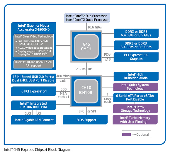
After the X3000s, Intel only designed one more chipset series with integrated graphics. The Intel GMA 4500 family was composed of four models, all of which used the same 10-EU architecture. Three versions were released for desktop chipsets. The slowest of these was GMA 4500, which operated at 533MHz. The other two were the GMA X4500 and X4500HD, both clocked at 800MHz. The primary difference between the X4500 and X4500HD was that the HD model featured full hardware acceleration of VC-1 and AVC, while the X4500 and GMA 4500 didn't.
The mobile variant was named GMA X4500MHD, and could be clocked at either 400 or 533MHz. Similar to the X4500HD, the X4500MHD supported full hardware acceleration of VC-1 and AVC.
Larrabee (2009)
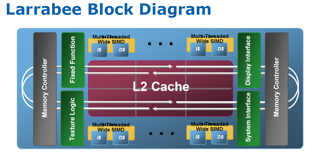
In 2009, Intel made another attempt to enter the graphics card business with Larrabee. Realizing that its immense understanding of x86 technology was the company's primary strength, Intel wanted to create a GPU based on the ISA. Development for Larrabee began with the original Pentium CPU, which Intel opted to modify in order to create the scalar unit inside of the GPU instead of starting from scratch. The old processor design was significantly revamped with new algorithms and Hyper-Threading technology to increase performance. Although the HTT used in Larrabee is similar to that in Intel's CPUs, Larrabee was capable of running four threads per core, rather than two.
For the vector processing unit, Intel essentially created an unusually large 512-bit floating-point unit composed of 16 individual elements capable of working as a single component or separate entities. This FPU was theoretically specified at over 10 times more throughput than comparable Nvidia GPUs from the same time period.
Larrabee would eventually be cancelled, though Intel continued developing the technology.
-
adamovera Archived comments are found here: http://www.tomshardware.com/forum/id-2839510/evolution-intel-graphics-i740-iris-pro.htmlReply -
LucaFire Great read :) Been waiting for something like this; no one really covers the history of Intel's graphics/integrated solutions.Reply -
bit_user ReplyLarrabee (2009)
No, it was theoretically specified at 2 TFLOPS, while Nvidia's GTX 285 could manage 708 GFLOPS. That's still impressive, but not > 10x.
Picture 11 of 20
...
This FPU was theoretically specified at over 10 times more throughput than comparable Nvidia GPUs from the same time period.
Real world performance of Larrabee was demonstrated at ~1 TFLOPS.
Sources:
■ https://en.wikipedia.org/wiki/Larrabee_(microarchitecture)■ https://en.wikipedia.org/wiki/List_of_Nvidia_graphics_processing_units#GeForce_200_series
Xeon Phi (2012)
Perhaps you meant to say "one of the world's faster computers, today"? According to top500.org, Sunway TaihuLight is #1, displacing Tianhe-2 (MilkyWay-2) to #2.
Picture 14 of 20
As a result of the high compute performance relative to power consumption, the Xeon Phi 31S1P was used in the construction of the Tianhe-2 supercomputer in 2013, which persists as the world's faster computer today.
Oh, and it's really not a GPU, though I guess it's fair to include, here. Without Xeon Phi, Larrabee ends up looking like a complete dead end. Plus, the whole HD graphics story is pretty uninteresting, with no huge changes from one generation to the next (aside from the addition of optional eDRAM).
BTW, you could've added the Knights Landing generation (https://en.wikipedia.org/wiki/Xeon_Phi#Knights_Landing), again showing the progression of the architecture started by Larrabee. With OmniPath, HMC, and motherboard socket compatibility, this made Xeon Phi start to look very interesting. -
bit_user Reply
Sorry, the only mainstream console to use ARM processors, so far, is Nintendo Switch. XBox 360, PS3, and the last 3 non-portable Nintendo's used variants of PowerPC, while XBox One and PS4 are using AMD (x86-64) APUs.19277885 said:The consoles run big GPU's along side ARM processors...
Though, it's definitely true that the bulk of consoles' compute power is contained in the GPU. Same is true for many phones, tablets, and even Intel's desktop CPUs.
Speaking of consoles, I've always wondered if the original Haswell-era GT3e was originally developed as a bid to win the XBox One design. Microsoft has always had a thing for a chunk of fast, on-chip memory. XBox 360 and XBox One both have it, while neither PS3 nor PS4 went that direction.
This is actually pretty close to what the Xeon Phi is. The latest generation (codename: Knights Landing) is sort of a hybrid between a CPU and GPU, where they took low-power general-purpose CPU cores from their Atom product line and made them much more GPU-like.19277885 said:The fastest computer's will be an array of co-processors including GPU's
Check out their Tesla products: https://en.wikipedia.org/wiki/List_of_Nvidia_graphics_processing_units#Tesla19277885 said:Nvidia has not had to whip out it's ... and show it off yet.
As you can see from that table, they've been going after server & cloud computing for about 10 years, now. Intel is trying to keep up, but you're also correct that Nvidia holds a substantial lead in both raw compute and energy-efficiency.
http://www.nvidia.com/object/tesla-supercomputing-solutions.html -
bit_user Reply
I'm not sure about AMD's older APU offerings, but Ryzen-based APUs will definitely stomp all over them, in this area.19378146 said:Think about it, Intel's GPU are actually the best for what it is intended for
