Ryzen Up: AMD to 3D Stack DRAM and SRAM on Processors
Get Tom's Hardware's best news and in-depth reviews, straight to your inbox.
You are now subscribed
Your newsletter sign-up was successful
AMD revealed at a recent high performance computing event that it is working on new designs that use 3D-stacked DRAM and SRAM on top of its processors to improve performance.
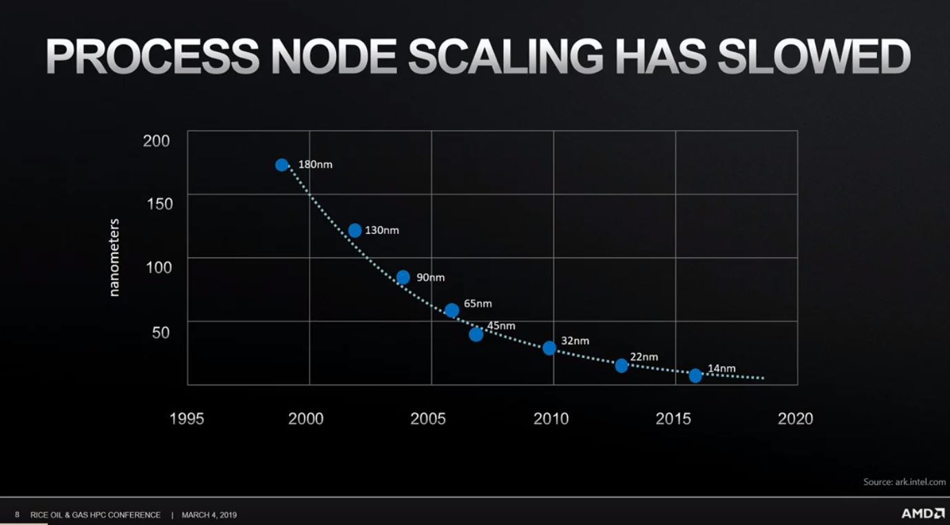
This innovative approach has become a necessity because silicon manufacturing isn't progressing at a rapid clip as it did during the heady days of Moore's Law, largely because of the extended and expensive development cycles for denser process nodes and a diminishing point of returns for higher clock speeds.
AMD, like many companies, has adjusted its strategy to deal with the difficult new reality, and in many respects, such as the company's move to chiplet-based architectures, AMD is leading the way. But other industry behemoths, like Intel, are also embracing multi-chip architectures while also moving on to the next new wave of innovation: 3D chip stacking.
Intel whipped the covers off its Foveros 3D chip stacking technology during its recent Architecture Day event and revealed it already has a leading-edge product ready to enter production. The package consists of a 10nm CPU and an I/O chip mated with TSVs (Through Silicon Via) that connect the die through vertical electrical connections in the center of the die. Intel also added a memory chip to the top of the stack using a conventional PoP (Package on Package) implementation.
Not to be left behind, AMD is also turning its eyes toward 3D chip stacking techniques, albeit from a slightly different angle. AMD SVP and GM Forrest Norrod recently presented at the Rice Oil and Gas HPC conference and revealed that the company has its own 3D stacking intiative underway.
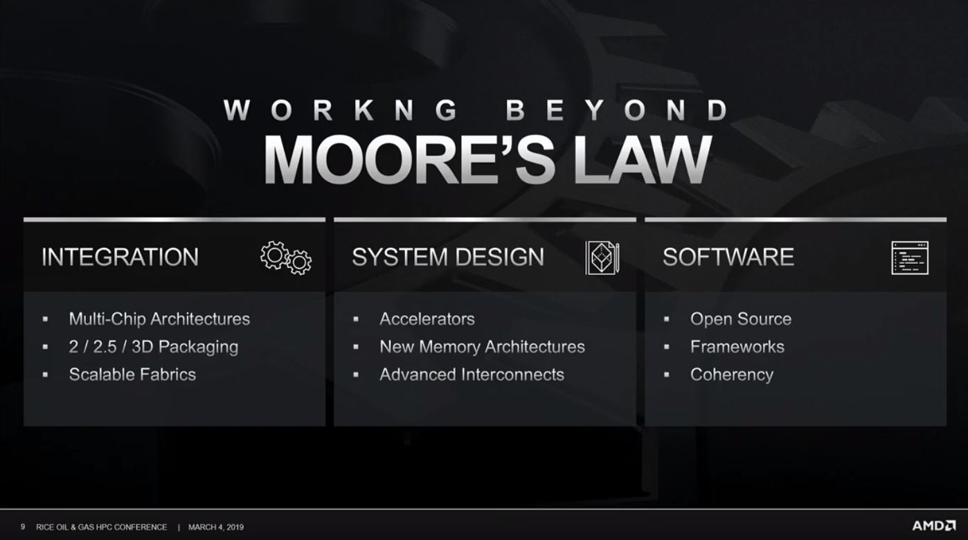
AMD's "Working Beyond Moore's Law" initiative involves developing several technologies to circumvent the diminishing point of returns from new process nodes. Norrod explained that AMD is using "every trick in the book" to circumvent the challenges because the two simple levers of density and frequency improvements have reached a diminishing point of returns. In some cases, frequency is even regressing.
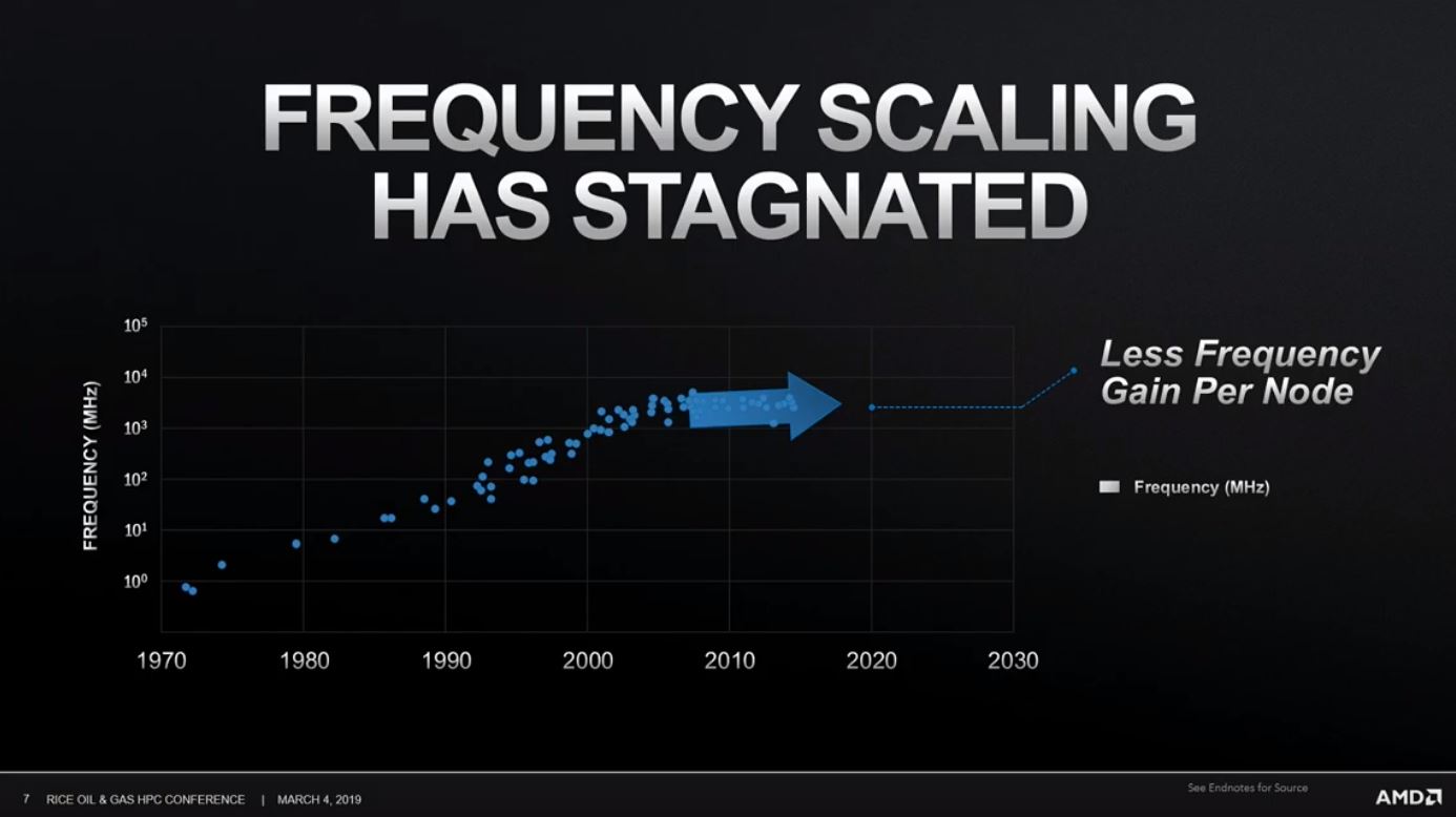
Norrod explained the challenges with frequency scaling: "The dirty little secret in the industry, though, over the last ten years that has stopped, and may now be regressing[...]As we continually shrink our processes now, we don't get any more frequency, and really with this next node, without doing extraordinary things, we get less frequency."
Get Tom's Hardware's best news and in-depth reviews, straight to your inbox.
Norrod didn't connect those statements to any specific node, such as TSMC's forthcoming 7nm node that will power its Ryzen 3000-series and EPYC Rome processors or the future 5nm node, but the underlying sentiment is clear: the industry can no longer rely upon increased frequency to drive performance improvements.
Norrod also explained that node density improvements are also slowing, and the industry is reaching the limits of scaling to larger die due to reticle limitations (~700mm2). Even multi-chip designs, like AMD's Threadripper processors, are running into space limitations due to the already-large size of the processor package.
Like other semiconductor vendors, AMD is working to move to 3D architectures to improve performance density. This approach also presents challenges due to thermal and power delivery constraints.
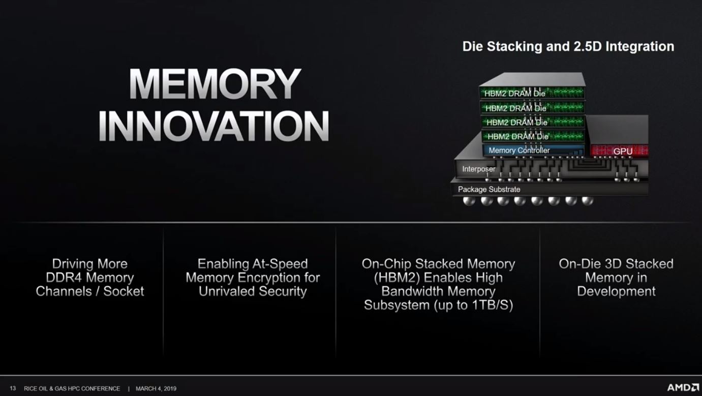
Nonetheless, AMD is moving to adopt new stacked memory architectures as it sees this as the most important step in the near term. AMD already stacks HBM2 memory next to its GPU die, meaning it resides in the same package as the processor, but the company plans to move to true 3D stacking in the near future.
Norrod explained that AMD is working on stacking SRAM and DRAM memory directly on top of computing components (like CPUs and GPUs) to expose even more bandwidth and performance.
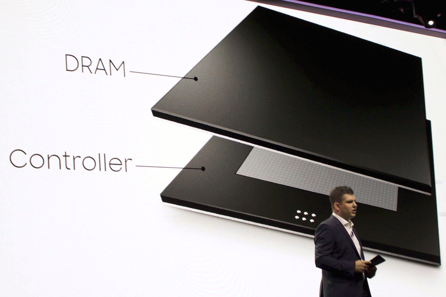
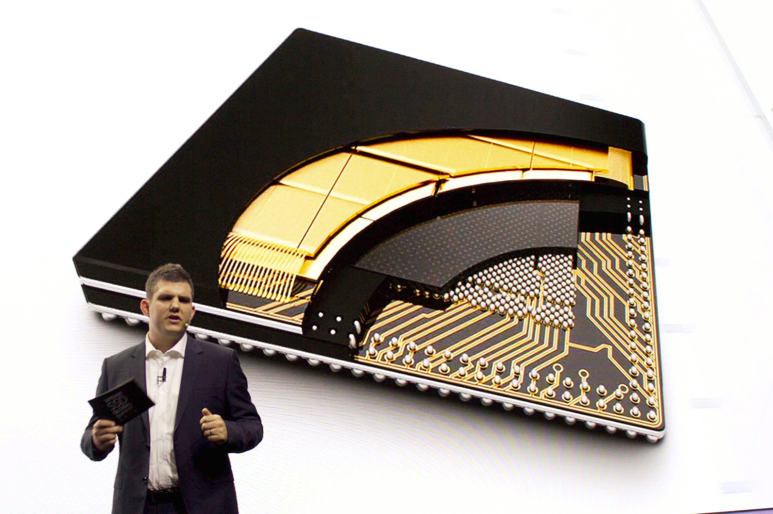
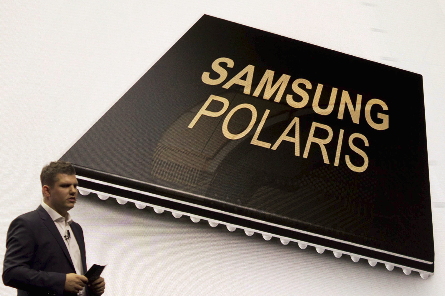
This on-die stacked memory approach would differ from normal package-on-package (PoP) implementations that simply place two finished packages atop one another, as seen above with a Samsung chip. In this example, the DRAM package connects through two additional rows of BGA connectors that ring the underlying chip. These BGA connectors carry the data transferred between the two chips. As with any standard design, the logic resides on the bottom of the stack due to its need for more connectors, but the two die are not connected directly. As such, the PoP approach provides the utmost in density, but it isn't the fastest option.
In contrast, true 3D stacking consists of two die (in this case, memory and a processor) placed on top of each other and connected through vertical TSV connections that mate the die directly together. These TSV connections, which transfer data between the two die at the fastest speeds possible, typically reside in the center of the die. That direct mating increases performance and reduces power consumption (all data movement requires power, but direct connections streamline the process). 3D stacking also affords density advantages.
Norrod didn't dive into more specifics of any designs under development, but this could prove to be a fundamental shift in AMD's processor design. Intel's fast pace of development with its own 3D Foveros technology could prove to be a defining moment for the industry, so it isn't surprising to hear that AMD is moving in this direction to keep pace. For now, details are under wraps, but we've followed up with AMD for more information.
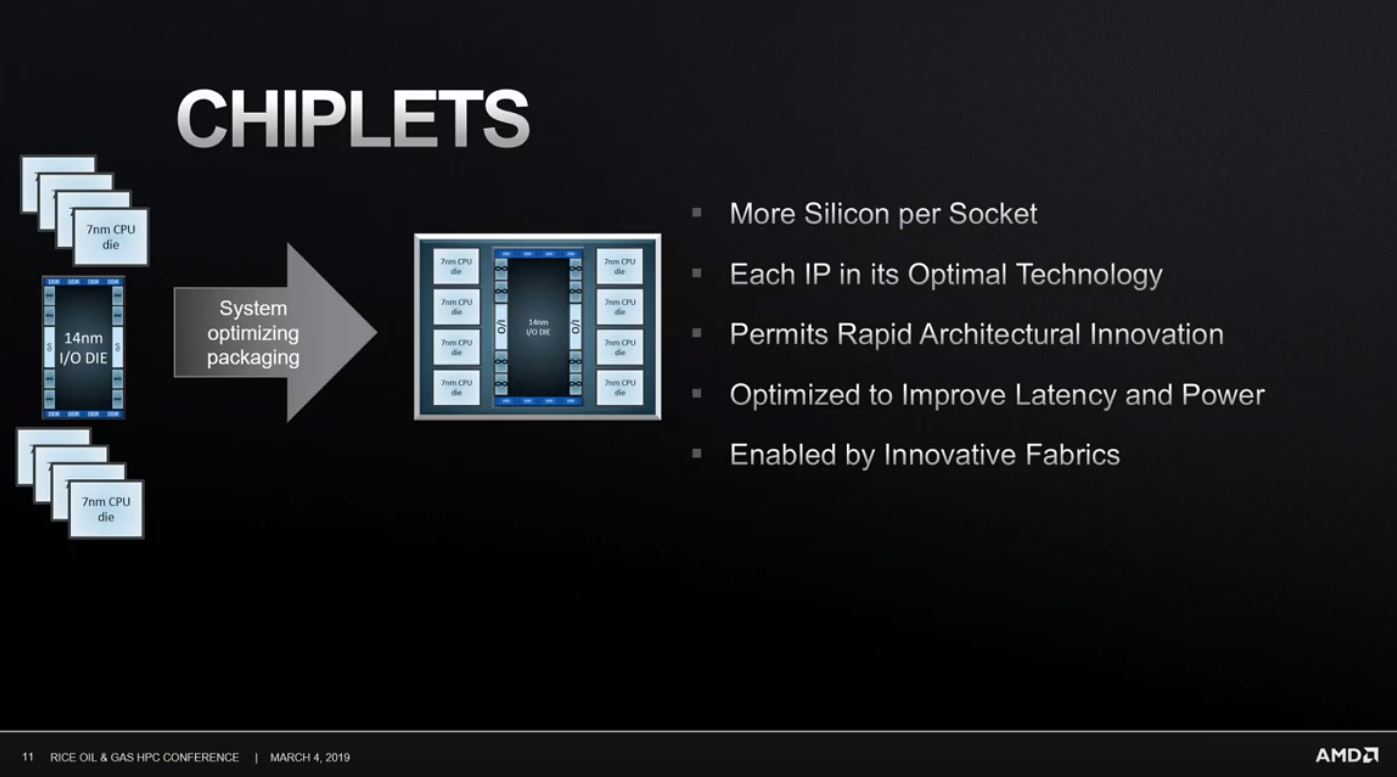
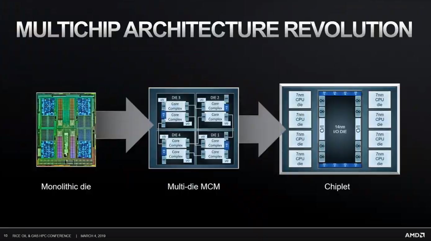
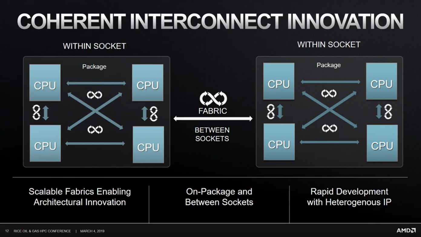
Norrod also expanded on the company's rationale behind the chiplet architecture, along with its work in developing new interconnects, like CCIX and Gen-Z, to improve performance at the system level. The newly-formed Compute Express Link (CXL) consortium recently announced a new interconnect, developed and contributed by Intel, that is designed to provide a cache-coherent interface between CPUs and other devices, like GPUs, FPGAs, and memory devices. This interface is said to mesh well with Gen-Z devices, so there should be some level of cooperation between the two standards bodies.
You can watch the full presentation below.
Image Credits: AMD

Paul Alcorn is the Editor-in-Chief for Tom's Hardware US. He also writes news and reviews on CPUs, storage, and enterprise hardware.
