AMD Announces the Instinct MI100 GPU, CDNA Breaks 10 TFLOPS Barrier
The Instinct MI100 is an FP64 Monster
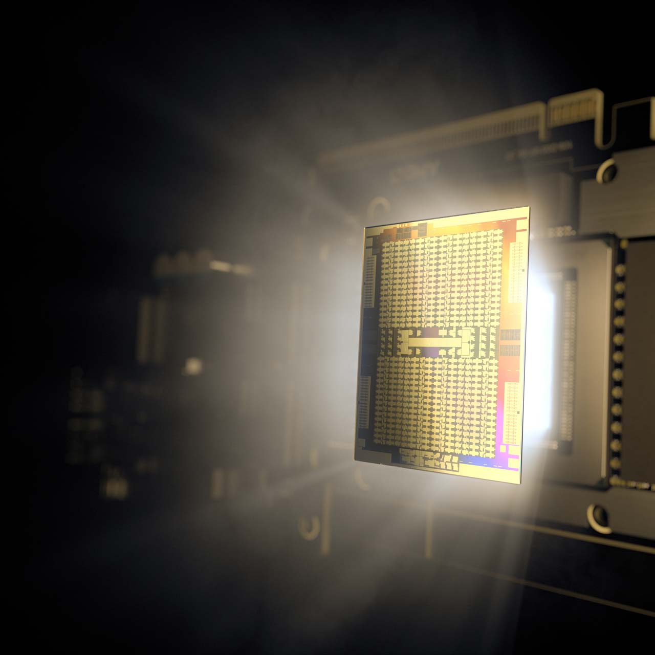
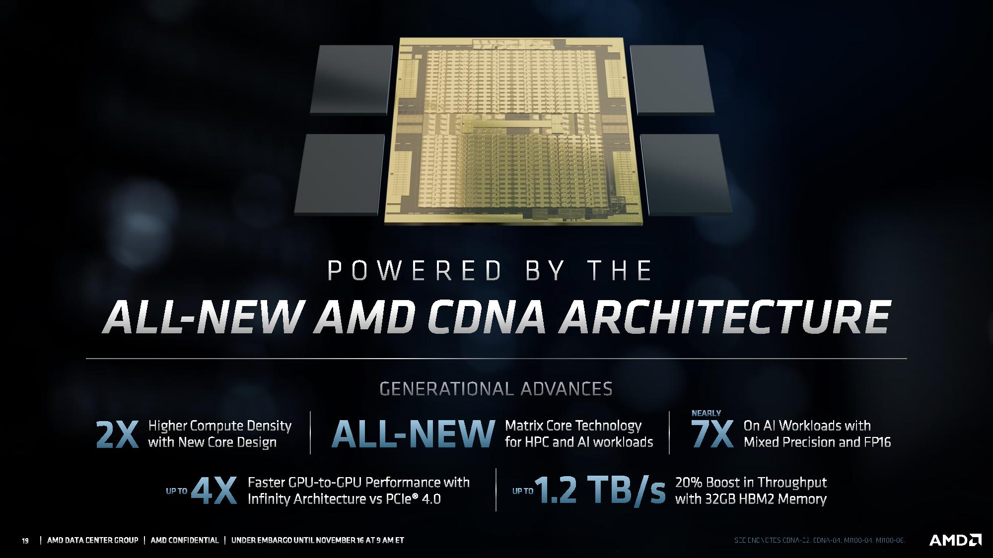
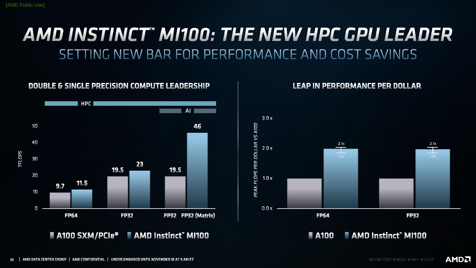
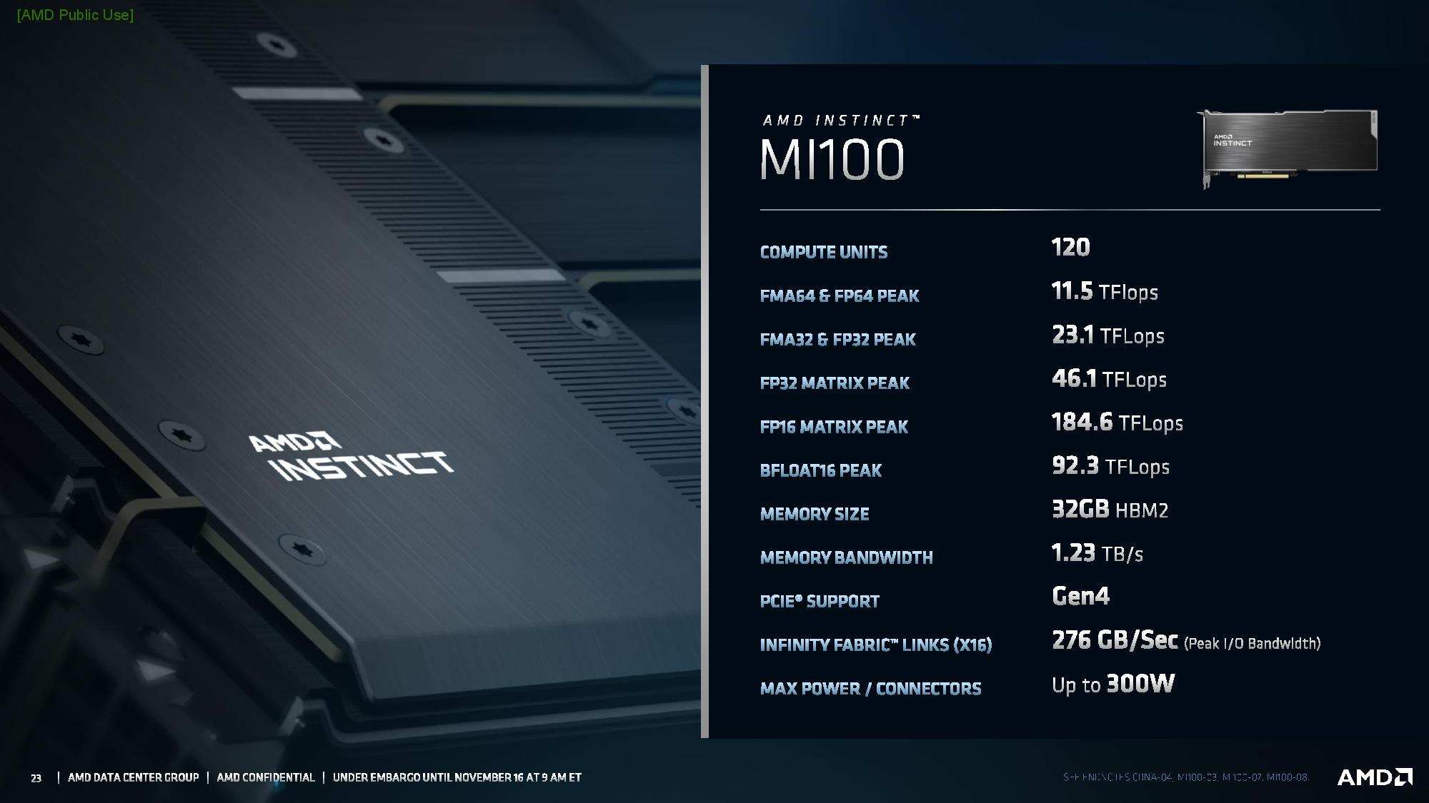
AMD announced its 7nm Instinct MI100 GPU today, along with a slew of design wins from the likes of Dell, HPE, and Supermicro. The Instinct MI100 marks the first iteration of AMD's compute-focused CDNA GPU architecture. The new architecture offers up to 11.5 TFLOPS of peak FP64 throughput, making the Instinct MI100 the first GPU to break 10 TFLOPS in FP64 and marking a 3X improvement over the previous-gen MI50. It also boasts a peak throughput of 23.1 TFLOPS in FP32 workloads, beating Nvidia's beastly A100 GPU in both of those categories, though it lags with other numerical formats.
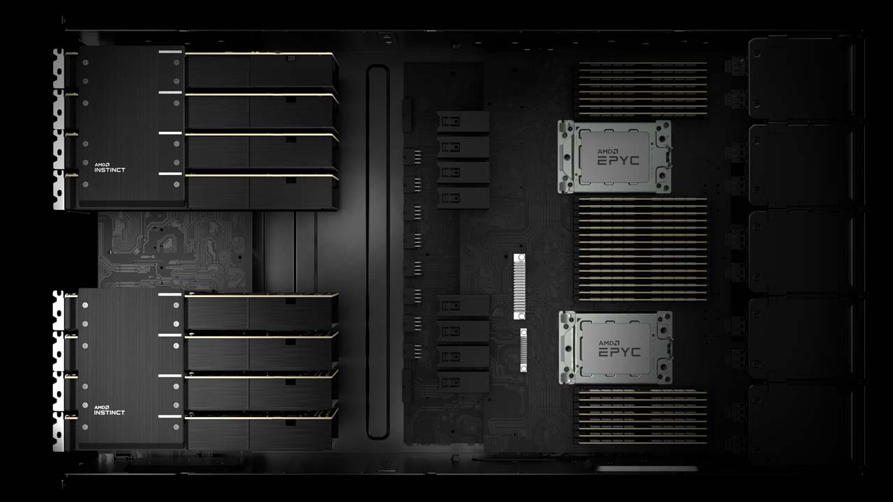
As expected from a data center GPU, the PCIe 4.0 card is designed for AI and HPC workloads and also supports AMD's second-gen Infinity Fabric, which doubles the peer-to-peer (P2P) I/O bandwidth between cards. This fabric allows the cards to share a unified memory address space with CPUs, a key advantage for AMD as it leverages its position as the only CPU vendor that is currently shipping data center-class GPUs. The cards boast up to 340 GB/s of aggregate throughput over three Infinity Fabric links and are designed to be deployed into quad-core hives (up to two per server), with each hive supporting up to 552 GB/s of P2P I/O bandwidth.
The Instinct MI100 also supports AMD's new Matrix Core technology that boosts performance in single- and mixed-precision matrix operations, like FP32, FP16, bFloat 16, INT8, and INT4. That tech boosts FP32 performance up to 46.1 TFLOPS.
The cards come with 32GB of HBM2 memory spread across four stacks that provide an aggregate of up to 1.23 TB/s of bandwidth. AMD claims the cards offer up to 1.8x to 2.1X more peak performance per dollar compared to Nvidia's A100 GPUs.
AMD also announced that its open source ROCm 4.0 developer software now has an open source compiler and unified support for OpenMP 5.0, HIP, PyTorch, and Tensorflow.
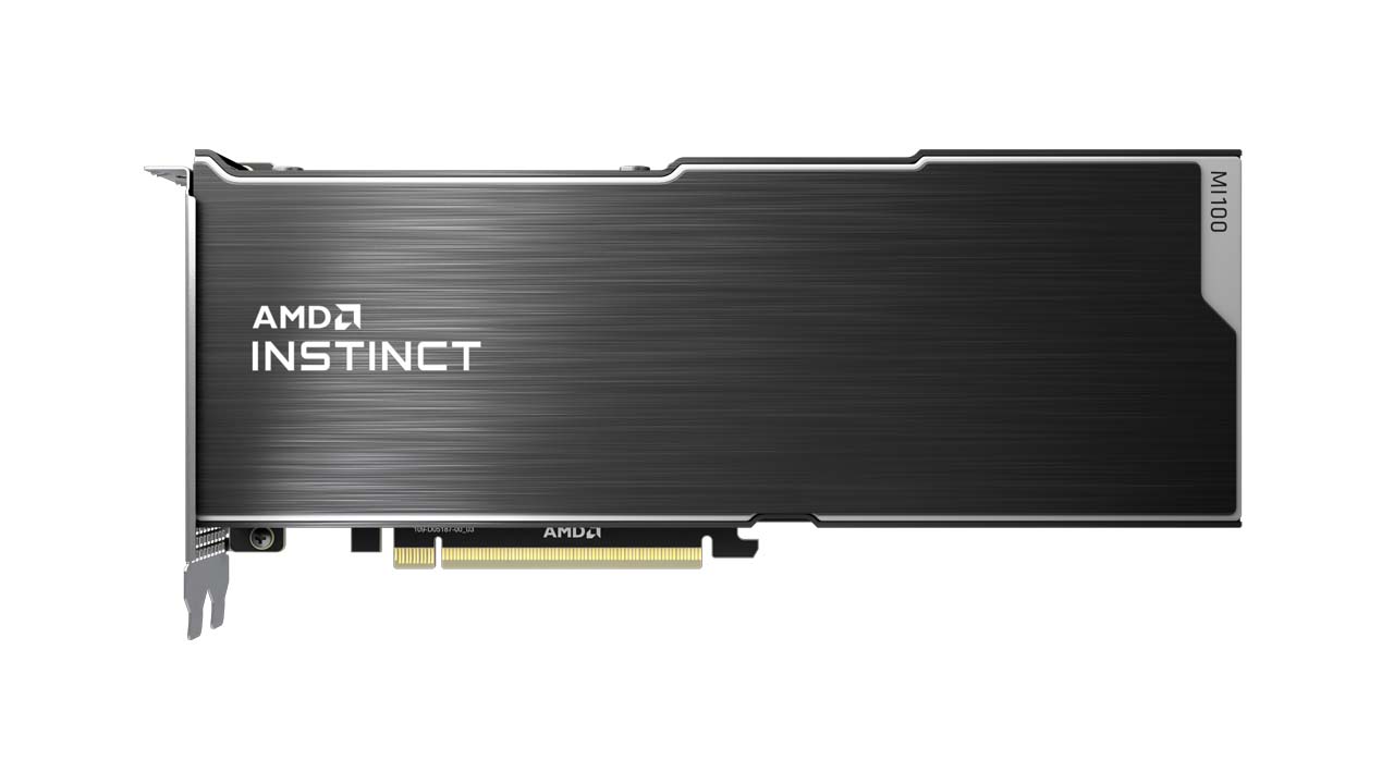
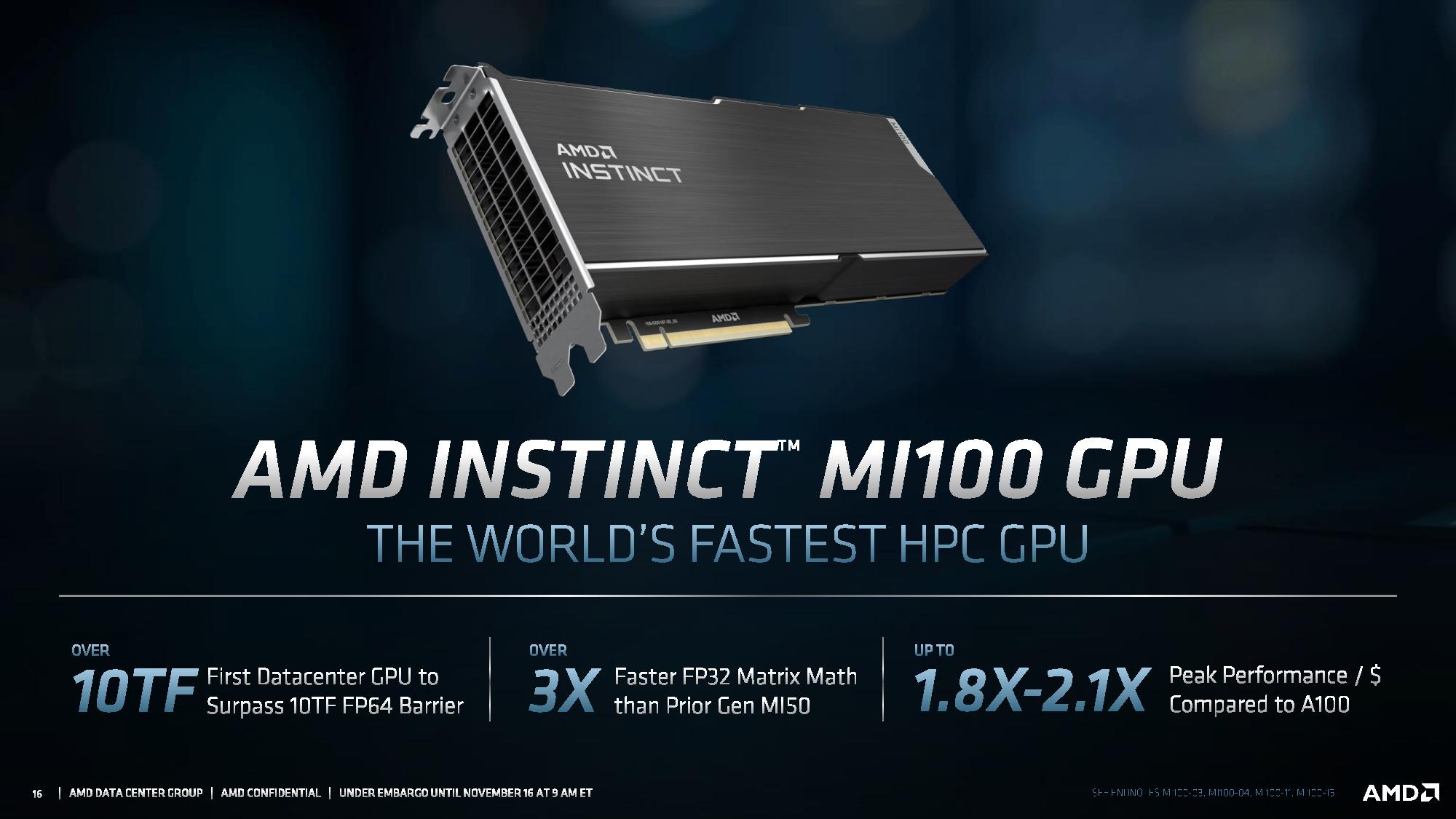
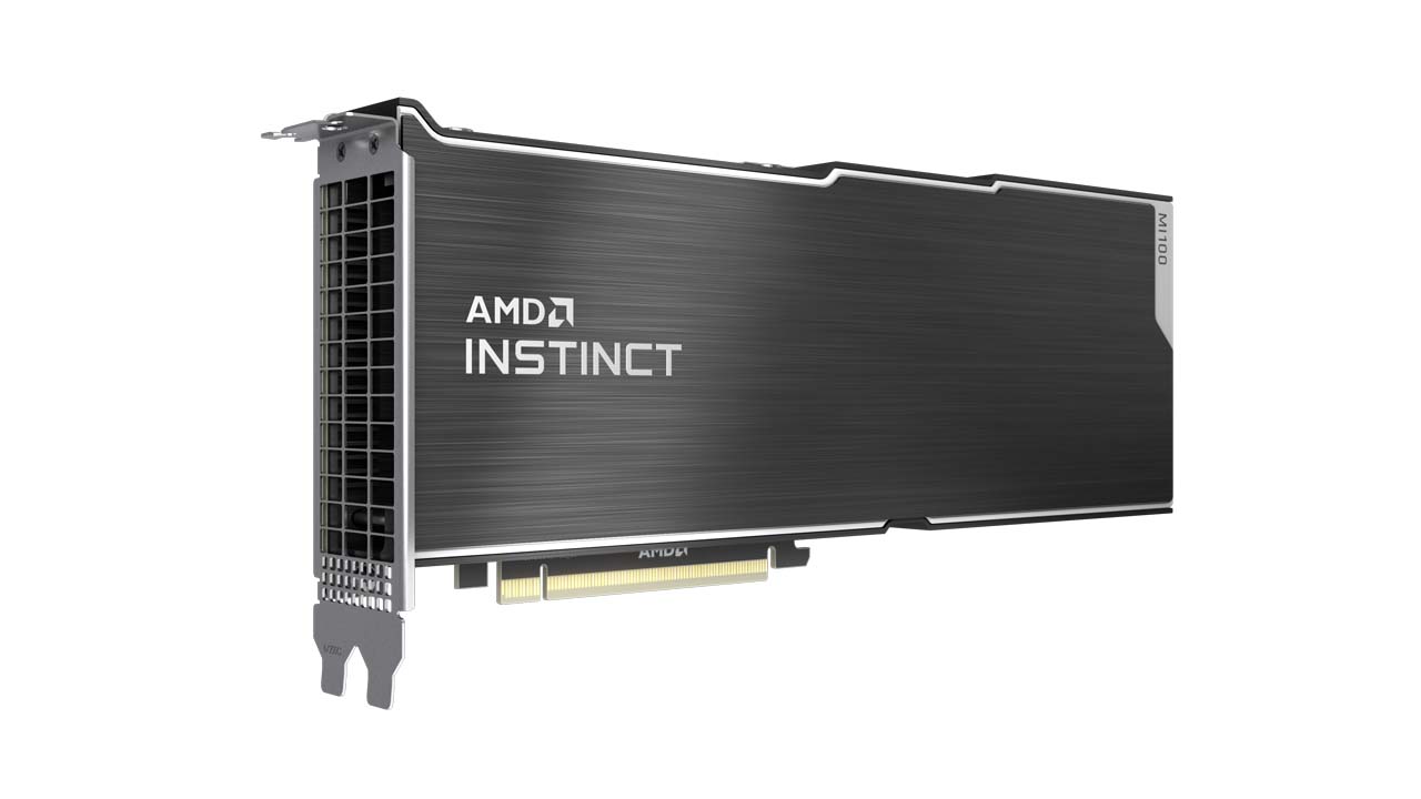
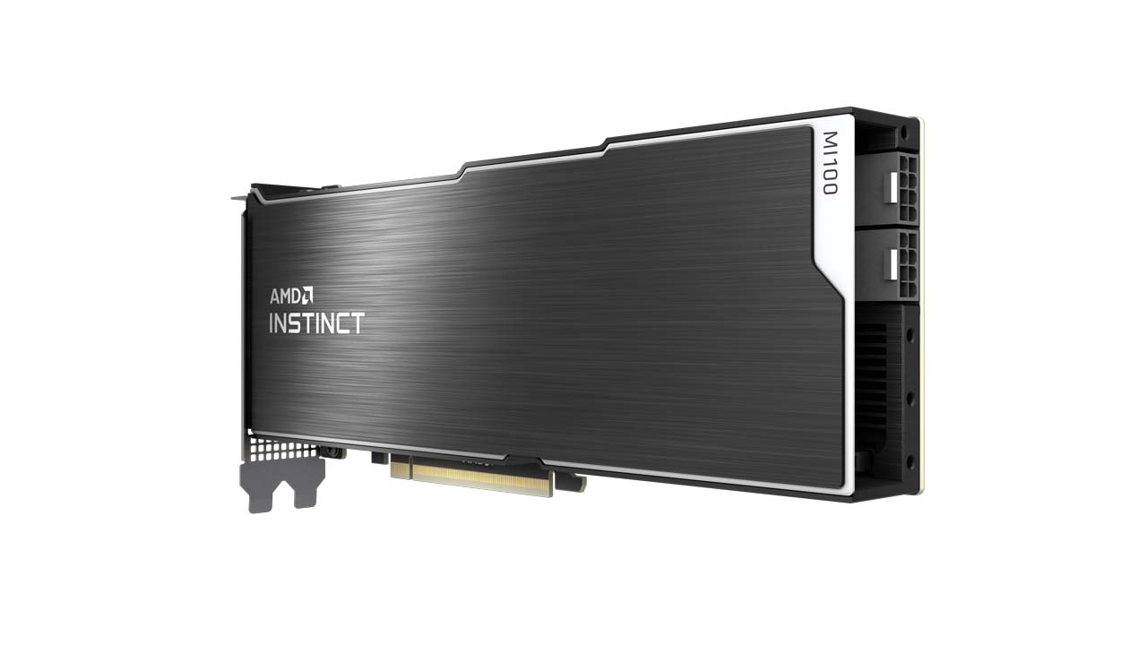
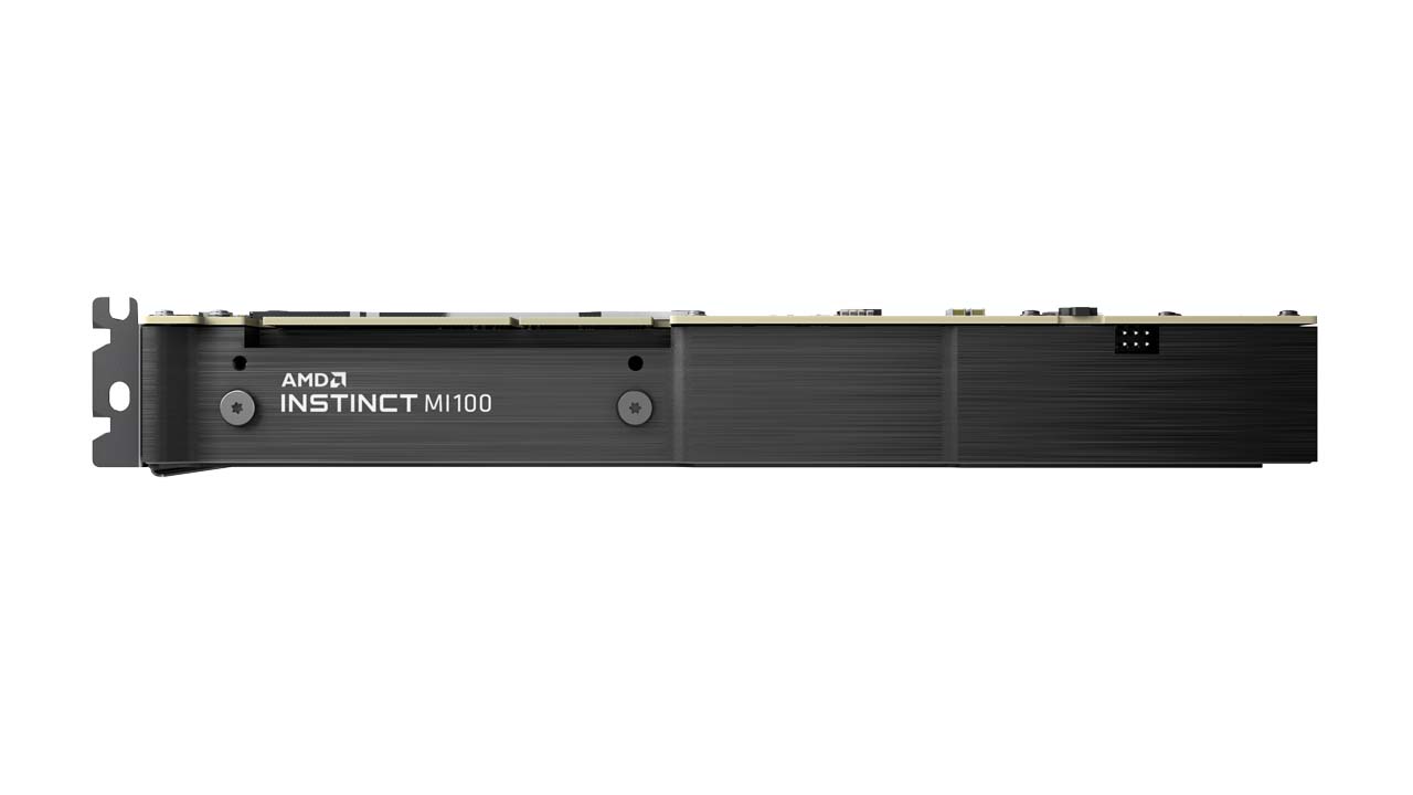
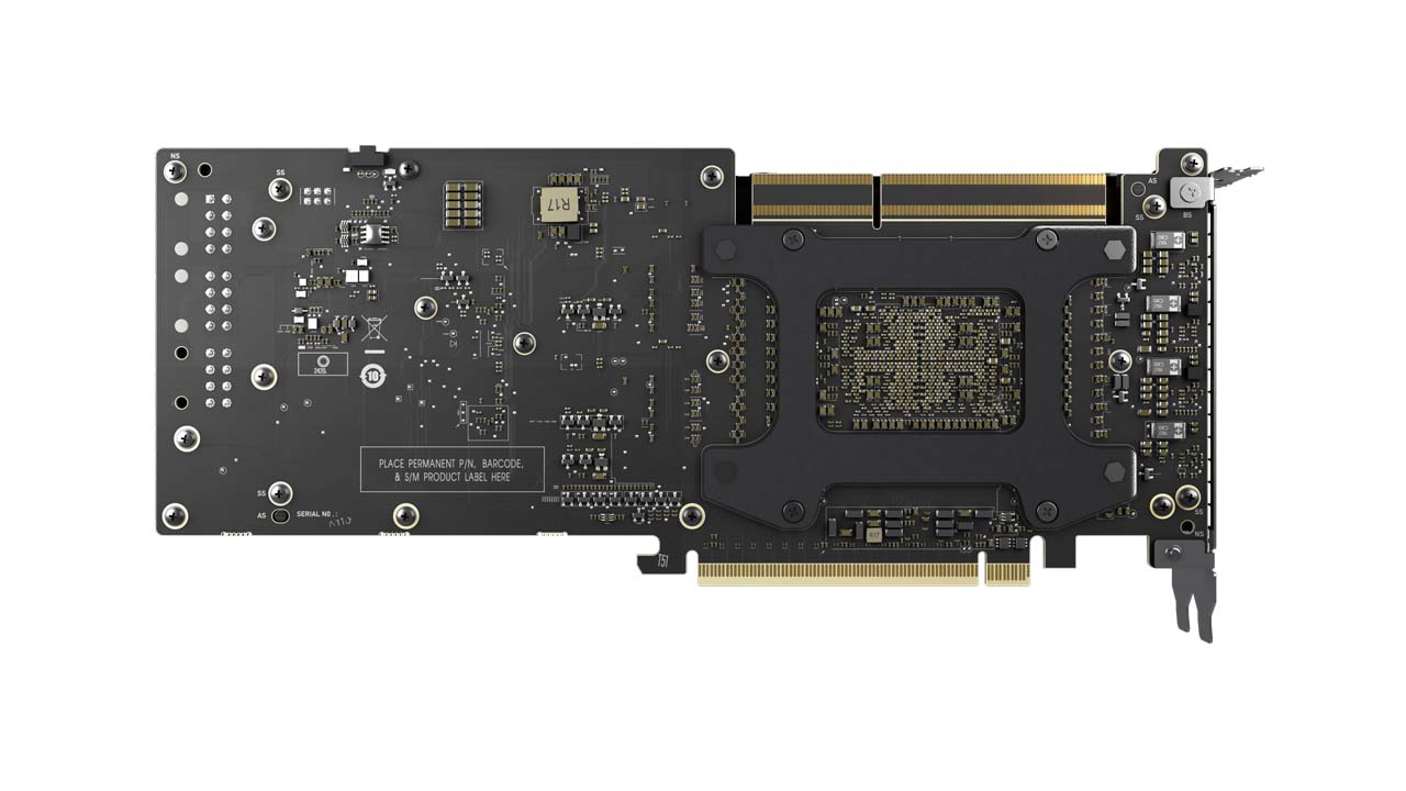
The card has a 300W TDP and comes in the standard PCIe Add-In Card (AIC) form factor with two eight-pin connectors for power. Given the data center focus, the card lacks display outputs, and the passively-cooled card has a rear I/O shield with a large mesh for efficient airflow.
| Row 0 - Cell 0 | Peak Clock | Stream Processors | TDP | HBM2 Memory | Memory Bandwidth | PCIe Interface |
| 7nm Instinct MI100 | 1502 MHz | 7680 (120 CU) | 300W | 32GB | 1.23 TB/s | 4.0 |
| 7nm Instinct MI50 | 1725 MHz | 3840 (60 CU) | 300W | 32GB | 1.024 TB/s | 4.0 |
| 7nm Nvidia A100 (PCIe) | 1410 MHz | 6912 | 250W | 40GB | 1.555 TB/s | 4.0 |
| 7nm Nvidia A1000 (HGX) | 1410 MHz | 6912 | 400W | 40GB | 1.555 TB/s | 4.0 |
AMD dialed back the MI100's peak clock rate to 1,502 MHz, down from 1,725 MHz with the previous-gen MI50, but doubled the number of compute units up to 120. The company also improved memory bandwidth to 1.23 TB/s.
Stay On the Cutting Edge: Get the Tom's Hardware Newsletter
Get Tom's Hardware's best news and in-depth reviews, straight to your inbox.
| Row 0 - Cell 0 | FP64 | FP32 | Matrix FP32 | Matrix FP16 | INT4/INT8 | bFloat16 |
| 7nm Instinct MI100 | 11.5 TFLOPs | 23.1 TFLOPS | 46.1 TFLOPS | 184.6 TFLOPS | 184.6 | 92.3 |
| 7nm Instinct MI50 | 6.6 TFLOPS | 13.3 TFLOPS | 13.3 TFLOPS | 26.5 TFLOPS | - | - |
| 7nm Nvidia A100 (PCIe) | 9.7 TFLOPS | 19.5 TFLOPS | 156 TFLOPS (Tensor) | 312 TFLOPS | 624 / 1,248 (Tensor core) | 624 / 1,248 (Tensor core) |
| 7nm Nvidia A1000 (HGX) | 9.7 TFLOPS | 19.5 TFLOPS | 156 TFLOPS (Tensor) | 312 TFLOPS | 1,248 (Tensor core) | 1,248 (Tensor core) |
The net effect of the improvements to the CDNA architecture (which we'll cover below) delivers a 1.74X gain in peak FP64 and FP32 throughput, and a whopping 3.46X improvement in matrix FP32 and 6.97X gain in matrix FP16. Those gains come courtesy of AMD's new Matrix Core technology that enhances the CUs with new Matrix Core Engines optimized for mixed data types.
AMD's MI100 beats the Nvidia A100 in peak FP64 and FP32 throughput by ~15%, but Nvidia's A100 still offers far superior throughput in matrix FP32, FP16 and INT4/INT8 and bFloat16 workloads.
AMD touts that the MI100 rivals the 6 Megawatt ASCI White, the world's fastest supercomputer in 2000 that weighed 106 tons and provided 12.3 TFLOPS of performance. In contrast, the MI1000 brings power down to 300W, weighs only 2.56 pounds, and dishes out 11.5 TFLOPS of performance.
AMD Instinct MI100 CDNA Architecture
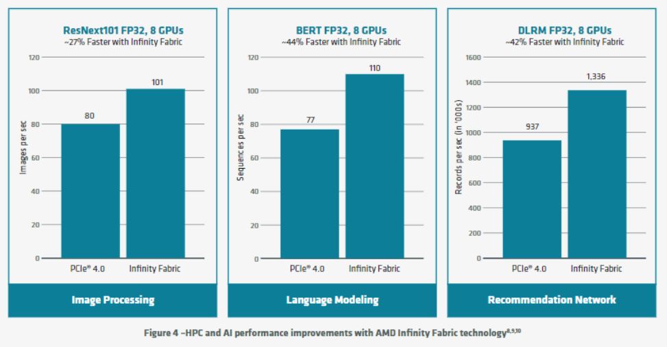
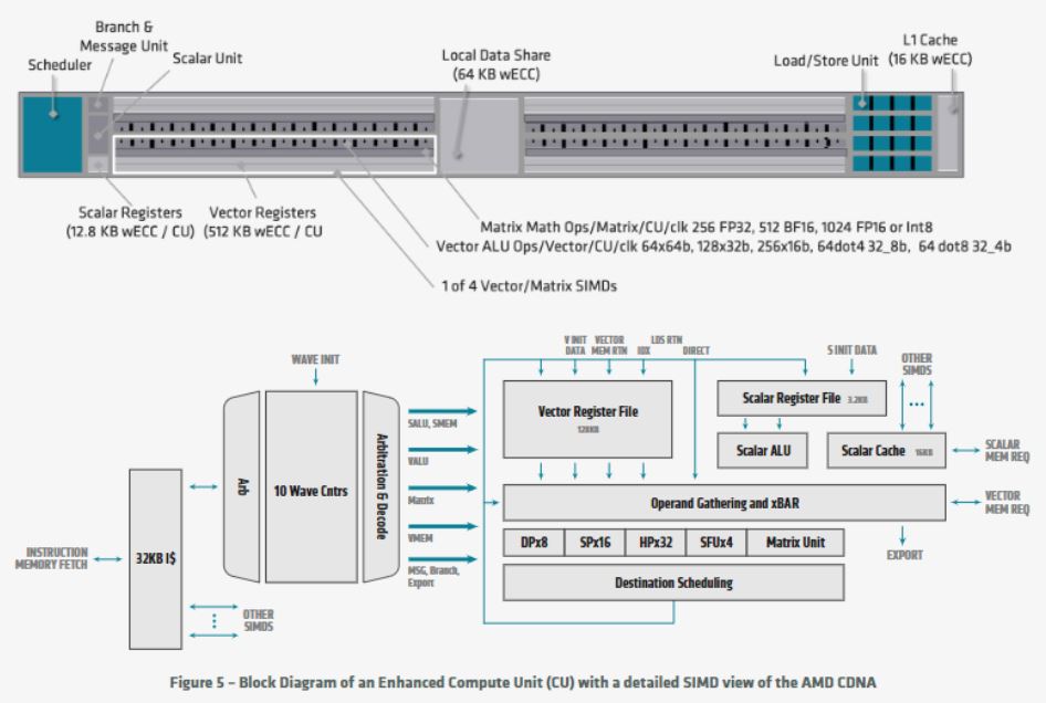

AMD split its graphics architectures into the RDNA platform for graphics-focused work (gaming) and CDNA for compute workloads (HPC/AI workloads) so it could deliver targeted enhancements to each respective architecture. Naturally, that means the CDNA designs come without many of the traditional fixed-function blocks needed for graphical work, like rasterization, tesselation, graphics caches, blending, and the display engine. The CDNA architecture does retain some logic for HEVC, H.264, and VP9 decoding, which is important for machine learning workloads that focus on object detection.
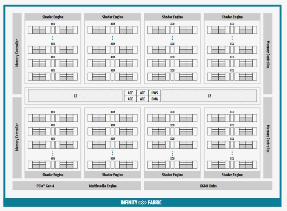
The 7nm Instinct MI100 marks the first iteration of the CDNA architecture and comes with a PCIe 4.0 interface that supports a 16 GT/s link (32 GB/s bi-directional) to the CPU. AMD isn't sharing the size of the 7nm die, which revision of 7nm it uses, or the transistor count, but we do know the 120 enhanced CUs are split into four compute engines. Each CU features a Matrix Core Engine that boosts computational throughput for various numerical formats, which AMD describes as:
"The classic GCN compute cores contain a variety of pipelines optimized for scalar and vector instructions. In particular, each CU contains a scalar register file, a scalar execution unit, and a scalar data cache to handle instructions that are shared across the wavefront, such as common control logic or address calculations. Similarly, the CUs also contain four large vector register files, four vector execution units that are optimized for FP32, and a vector data cache. Generally, the vector pipelines are 16-wide and each 64-wide wavefront is executed over four cycles."
"The AMD CDNA architecture builds on GCN’s foundation of scalars and vectors and adds matrices as a first class citizen while simultaneously adding support for new numerical formats for machine learning and preserving backwards compatibility for any software written for the GCN architecture. These Matrix Core Engines add a new family of wavefront-level instructions, the Matrix Fused Multiply-Add or MFMA. The MFMA family performs mixed-precision arithmetic and operates on KxN matrices using four different types of input data: 8-bit integers (INT8), 16-bit half-precision FP (FP16), 16-bit brain FP (bf16), and 32-bit single-precision (FP32). All MFMA instructions produce either 32-bit integer (INT32) or FP32 output, which reduces the likelihood of overflowing during the final accumulation stages of a matrix multiplication."
The matrix execution unit handles MFMA instruction and reduces the number of register file reads because many matrix multiplication input values are re-used.
The shared 8MB L2 cache is physically partitioned into 32 slices (twice as many as MI50) and is 16-way set associative. Overall, the 32 slices deliver up to 6TB/s of aggregate throughput. The memory controllers support 4- or 8-high stacks of ECC HBM2 at 2.4 GT/s, with an aggregate theoretical throughput of 1.23 TB/s. That's 20% faster than prior-gen models.
AMD Second-Gen Infinity Fabric
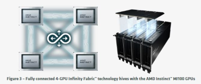

AMD's CPU-to-GPU Infinity Fabric has proven to be a key advance that has helped the company win numerous exascale contracts. This technology enables shared memory/cache coherency between CPUs and GPUs to reduce latency, boost performance, and reduce power draw by reducing the amount of data movement inside the system.
The second-gen Infinity Fabric links operate at 23 GT/s and are 16-bit wide, just like with the previous-gen, but the latest revision supports a third link to enable quad-GPU configurations. This new design works best in quad-GPU hives, with a typical two-socket server supporting two hives - one per CPU.
These hives operate in a fully-connected topology, whereas the previous accelerators used a ring topology. The new topology boosts performance during all-reduce and scatter/gather operations, among others.
Overall, AMD's second-gen Infinity Fabric dishes out twice the peer-to-peer (P2P) I/O bandwidth, with up two 340 GB/s of throughput per card (with three links). A quad-GPU hive provides up to 552 GB/s of P2P I/OP throughput, showing that the fabric doesn't scale linearly.
The fully-connected topology and shared address space is a key advantage for AMD over Nvidia and has led to several notable exascale supercomputing contracts. Notably, Nvidia has yet to announce an exascale supercomputer contract, but AMD's accelerators have already enjoyed broad uptake in the supercomputing and HPC realms.
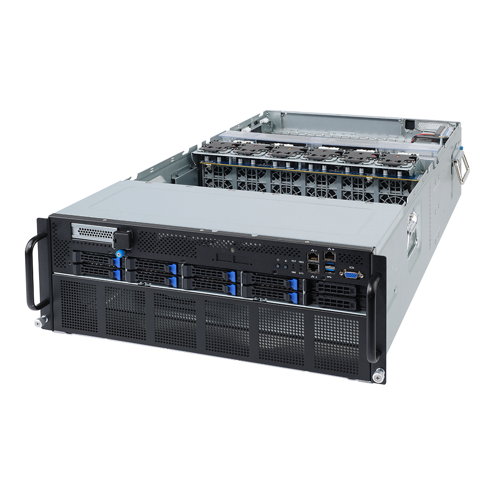
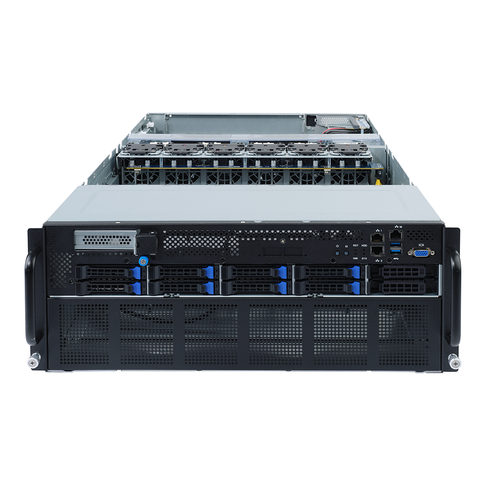
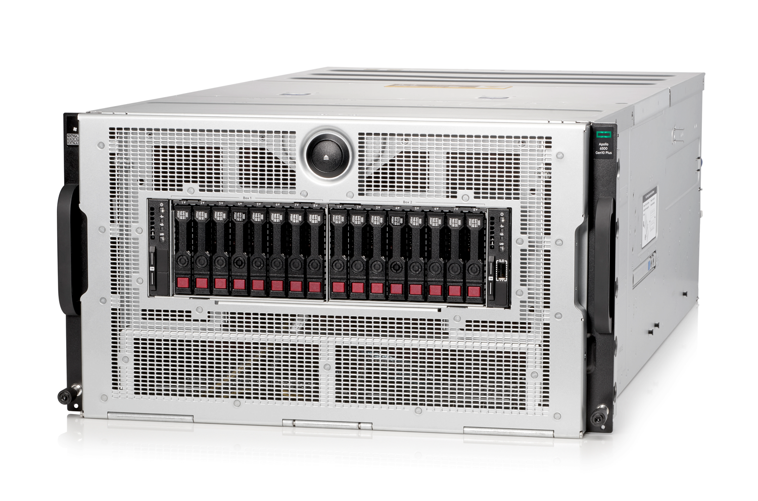
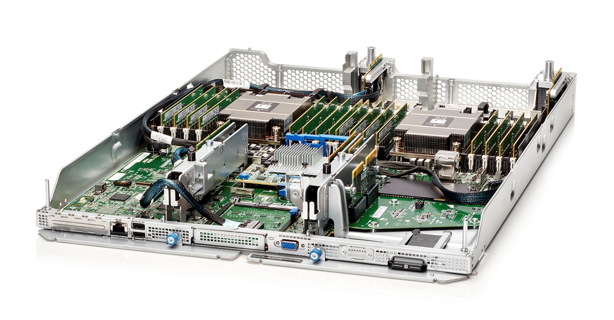
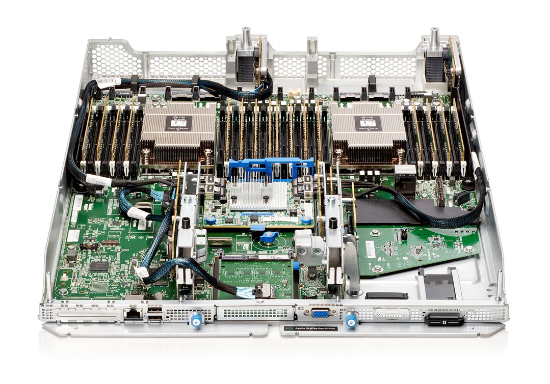
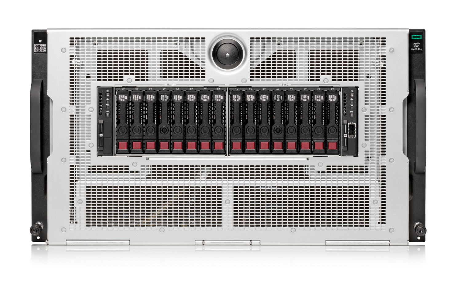
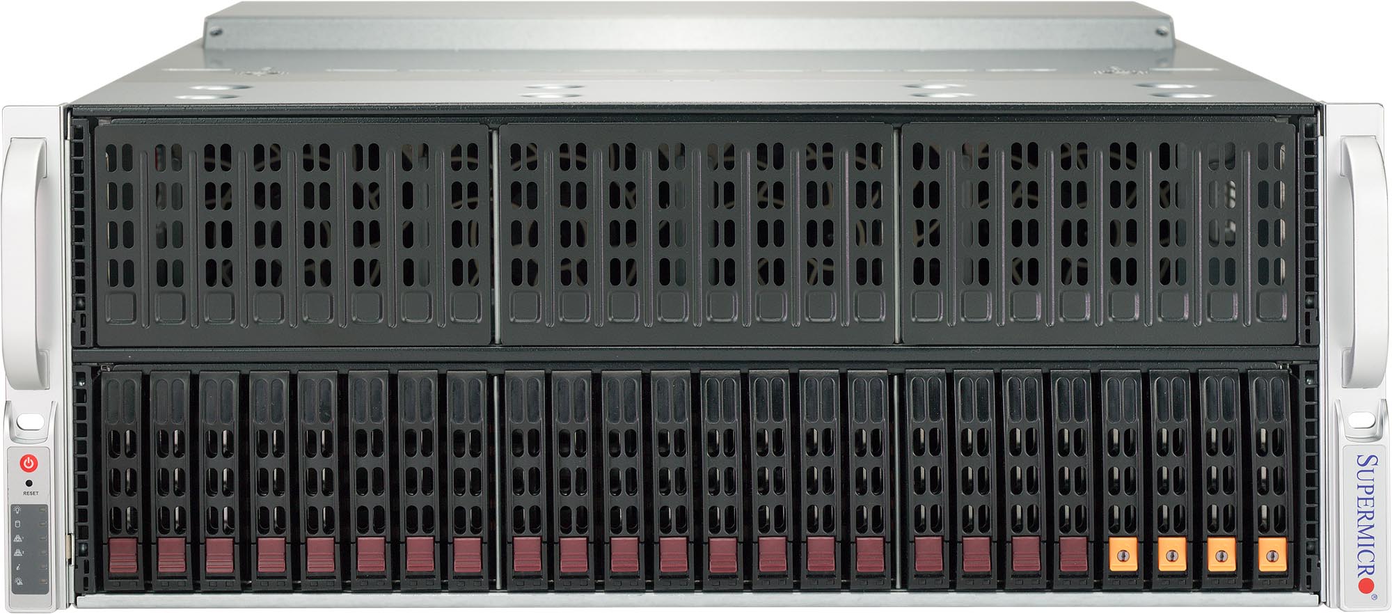
AMD also announced that fully-qualified OEM systems with the Instinct MI100 will be available from major OEMs, like Dell, Gigabyte, HPE, and Lenovo, by the end of the year.

Paul Alcorn is the Managing Editor: News and Emerging Tech for Tom's Hardware US. He also writes news and reviews on CPUs, storage, and enterprise hardware.
-
thGe17 First of all: the A100 values are a little bit mixed up.Reply
With Tensor Cores:
bfloat16 or FP16 = 312 TFlops (with sparsity up to 624 TFlops)
TF32 = 156 TFlops (with sparsity up to 312 TFlops)
("FP32-like/precision equivalent" matrix ops for training)
INT8 = 624 TOPS (with sparsity up to 1248 TOPS)
Additionally the regular base FP64 performance is 9.7 TFlops, but additionally Ampere can calculate FP64 MMA-ops via Tensor Cores in full precision and they have extended their CUDA-X libs for easy handling, therefore the resulting FP64 for a lot of (or even most?) workloads should be much higher than 9.7 TFlops FP64.
In the end it seems that MI100 is no match for Ampere, especially not with regards to AI workloads. -
TCA_ChinChin Reply
I guess, but its still based on the usage of tensor in addition to the raw FP performance. If you're after raw FP performance, the mi100 seems to have higher numbers on paper. The amount of FP workloads that can be increased by specific use of CUDA and Nvidia's various ML libraries does seem to be quite large, but that's still something up to the individual company/researcher to determine if its useful so it's still useful to compare the "base" FP64/32 results.thGe17 said:First of all: the A100 values are a little bit mixed up.
With Tensor Cores:
bfloat16 or FP16 = 312 TFlops (with sparsity up to 624 TFlops)
TF32 = 156 TFlops (with sparsity up to 312 TFlops)
("FP32-like/precision equivalent" matrix ops for training)
INT8 = 624 TOPS (with sparsity up to 1248 TOPS)
Additionally the regular base FP64 performance is 9.7 TFlops, but additionally Ampere can calculate FP64 MMA-ops via Tensor Cores in full precision and they have extended their CUDA-X libs for easy handling, therefore the resulting FP64 for a lot of (or even most?) workloads should be much higher than 9.7 TFlops FP64.
In the end it seems that MI100 is no match for Ampere, especially not with regards to AI workloads.
Seems like AMD's making strides, but Nvidia will still have the upper hand with their years of investment into CUDA and various ML learning workloads. It's gonna take AMD more that just having decent hardware to make up the difference. -
thGe17 Yes, so it seems. Additonally nVidia announced its upgraded A100 with 80 GiB HBM2E with 2 TB/s bandwidth and additionally Infiniband 400G. Looks as if they have only waited for AMD to make the first move. ;-)Reply
So hopefully AMD will have more luck with its new cards than with the last Gen, which looked also promising on paper.