AMD Patents Chiplet Design To Build Colossal GPUs
After chiplet-based CPUs, chiplet-based GPUs make sense, right?
Get Tom's Hardware's best news and in-depth reviews, straight to your inbox.
You are now subscribed
Your newsletter sign-up was successful
AMD jumped over to using a chiplet-based CPU design with the introduction of Zen 2 in the Ryzen 3000 series CPUs, enabling the chipmaker to cram more cores into a single CPU. Now, a new patent appears to reveal that AMD wants to do the same thing with GPUs (via ComputerBase).
Breaking Through the Performance Barrier
On the face of it, this move certainly makes sense. As you increase die sizes, yields tend to drop drastically due to defects in the silicon, leading to costly losses that impact prices. Semiconductor manufacturing equipment also has a reticle size limit, which essentially creates a barrier beyond which it simply isn't possible to make a bigger GPU. Coupled with the state of the process node (TSMC is currently at 7nm), there is a performance ceiling that foundries simply cannot manufacture beyond.

However, breaking the big silicon die into multiple little ones addresses those pain points. But things aren't quite this simple, and AMD's patent explains why this hasn't been done yet.
Article continues belowThe long and short of it is that parallelism in GPU compute workloads is difficult to span across multiple chiplets. CPU workloads are big and do not require a lot of communication between each other -- which is why it's comparatively easy to make a chiplet-based CPU.
Make it Look Like One, Big, Monolithic GPU
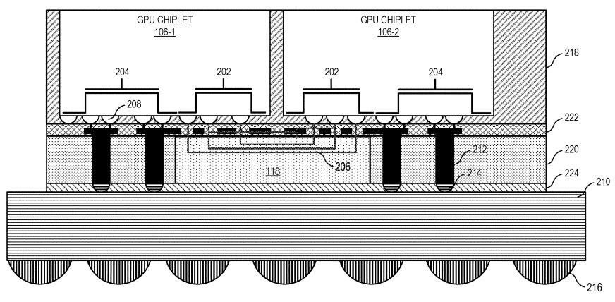
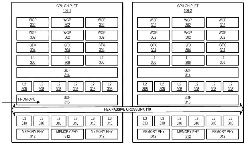
But GPU workloads are tiny, which leads to lots of traffic overhead on the internal communication fabrics. To solve this, AMD's approach uses a high-bandwidth interconnect to facilitate communication between chiplets -- AMD calls this crosslink an HBX. At the physical level, this will look much like the interposer of Zen 3 CPUs, except that on an electrical level, it is connected with a focus on L3 cache synchronization to account for the parallel workload.


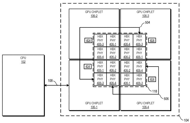
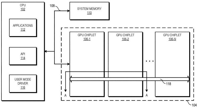
The design is proposed such that the CPU is connected to the first GPU chiplet, and one passive interconnect ties the L3 cache and other channels together between chiplets. This means that as far as the CPU is concerned, it communicates with one big GPU rather than a bunch of little GPUs.
A single controller that communicates with the smaller GPUs isn't a viable solution. The parallel workloads would generate too much traffic, and active switching would quickly create a (latency) bottleneck -- or demand far too big of a controller. As such, AMD proposes that a chiplet-based GPU needs a simple electrical path to be tied together to look like one big GPU, rather than a bunch of little ones addressed through a controller.
Get Tom's Hardware's best news and in-depth reviews, straight to your inbox.

The beauty of this GPU model is that it remains compatible with existing coding languages, and the GPU model doesn't change from the developers' point of view. A few things will need to be adjusted in the driver, naturally, to account for the new architecture, but existing software should run without any major changes.
The patent also goes on to explain that the layout of the chiplet-based GPU does not have to take form with four chiplets. Other configurations, die sizes and shapes may be welcome depending on the client's needs, with even pentagon-shaped dies as an option. Naturally, the design should be scalable, though symmetry between the chiplets would be a limitation.
Sounds Great. When is it Coming?
As great as it all sounds, we don't want to get your hopes up for such a product to come out anytime soon. SLI and Crossfire died because getting multiple GPUs to work together across different cards is a pain, and even with AMD's proposed solution of bringing the GPU chiplets closer together with a high-bandwidth interconnect, there is still a lot of work to be done.
Chances are that if this manifests into a real-world product, it will first happen on a research-level scale, being aimed at supercomputers or scientific-purpose GPUs for users with high GPU power needs in single workstations. Such a ludicrous amount of GPU horsepower will likely need to be coupled to HBM memory just to keep up, so it's likely that you can rule out consumer products for some time to come.
All that being said, it's also very possible that this will never become a thing. Tech companies file a lot of patents, and most of them never end up being used.
Niels Broekhuijsen is a Contributing Writer for Tom's Hardware US. He reviews cases, water cooling and pc builds.
-
JamesSneed This will certainly become a thing used for HPC. Will it ever filter down to gamers? Maybe but unlikely.Reply -
The Commander Wasn't Ada Lovelace/Hopper('RTX 4k') gonna use a multi-GPU chiplet design, too?Reply
Look at how well the chiplets have worked in consumer CPUs.Look at the big.LITTLE aspect of ARM, too.JamesSneed said:This will certainly become a thing used for HPC. Will it ever filter down to gamers? Maybe but unlikely. -
neojack thanks for the articleReply
how does this compare to the already existing infinity fabric that exists inside the pro M50/M60 instinct GPUs ? -
Koen1982 I wonder why Nvidia never implemented something similar, just make a chip that have a x1 of x2 lane connection on the PCIe connector and connect them together with an nvlink.Reply -
InvalidError I wish companies would quit patenting the obvious. Dividing large designs into multiple chips for costs and manufacturability reasons has been around for decades - the Voodoo 2 was a multi-chip GPU with each chip handling a specific chunk of the rendering pipeline. This is little more than AMD's flavor of the same principles (partition a design along logical/practical boundaries) applied to its own GPUs.Reply -
digitalgriffin They called me crazyReply
But I said this was going to happen over 5 years ago. The biggest hindrance was the data synchronizing and that would be solved by infinity cache like interfaces. Things went a lot slower than I predicted however. I knew that data coherency was a tough nut to crack.
We'll see if my last prediction comes true:
One APU:
CPU 8/16 core/thread chiplette
IO Die chiplette
iGPU chiplette
4GB HBM memory reserved by drivers as a cache. -
digitalgriffin ReplyKoen1982 said:I wonder why Nvidia never implemented something similar, just make a chip that have a x1 of x2 lane connection on the PCIe connector and connect them together with an nvlink.
They are working on it. First they said it couldn't be done two years ago.
Just recently they announced there is a delay in implementation. So you know they changed their mind. -
jkflipflop98 Replydigitalgriffin said:They are working on it. First they said it couldn't be done two years ago.
Just recently they announced there is a delay in implementation. So you know they changed their mind.
I'd like to see a link to that quote. Being as Nvidia owns all 3DFX's technology, they already own multiple designs like this from decades ago. -
spongiemaster Reply
Interesting that they said 2 years ago it couldn't be done, when they released a research paper 3.5 years ago that said it could be done.digitalgriffin said:They are working on it. First they said it couldn't be done two years ago.
Just recently they announced there is a delay in implementation. So you know they changed their mind.
https://research.nvidia.com/sites/default/files/publications/ISCA_2017_MCMGPU.pdf
From the conclusion:
"We show that with these optimizations, a 256 SMs MCM-GPU achieves 45.5% speedup over the largest possible monolithic GPU with 128 SMs. Furthermore, it performs 26.8% better than an equally equipped discrete multi-GPU, and its performance is within 10% of that of a hypothetical monolithic GPU that cannot be built based on today’s technology roadmap."
Here's another link from September 2019 that says they have multiple design solutions they could implement if they became more cost effective:
Nvidia has “de-risked” multiple chiplet GPU designs – “now it’s a tool in the toolbox”
Note this is for compute tasks only, not gaming. That has always been the crux of the issue. Multi-GPU works great for many compute tasks, but the complete death of any form of SLI in gaming shows how much more sensitive gaming is to the latencies and coherency between multiple GPU's. Chiplets may get us closer, but there is no indication from anyone yet, that it is actually the solution. -
digitalgriffin Replyspongiemaster said:Interesting that they said 2 years ago it couldn't be done, when they released a research paper 3.5 years ago that said it could be done.
https://research.nvidia.com/sites/default/files/publications/ISCA_2017_MCMGPU.pdf
From the conclusion:
"We show that with these optimizations, a 256 SMs MCM-GPU achieves 45.5% speedup over the largest possible monolithic GPU with 128 SMs. Furthermore, it performs 26.8% better than an equally equipped discrete multi-GPU, and its performance is within 10% of that of a hypothetical monolithic GPU that cannot be built based on today’s technology roadmap."
Here's another link from September 2019 that says they have multiple design solutions they could implement if they became more cost effective:
Nvidia has “de-risked” multiple chiplet GPU designs – “now it’s a tool in the toolbox”
Note this is for compute tasks only, not gaming. That has always been the crux of the issue. Multi-GPU works great for many compute tasks, but the complete death of any form of SLI in gaming shows how much more sensitive gaming is to the latencies and coherency between multiple GPU's. Chiplets may get us closer, but there is no indication from anyone yet, that it is actually the solution.
You may be right. It might have been 3.5 years ago. However I distinctly remember them originally saying "It wasn't feasible" before that. Maybe that was fodder to mislead AMD. But AMD was already working on a solution by then.
You have to remember the first hints of a possibility of a MCM design showed up over 5 years ago. Their hints on the roadmap were scalable design with heterogeneous architecture. I knew the tech was already there based on Fiji's interposer (Fury). I knew it was possible to break up a chip based on the functional block design if they could be coherent with the pixel data across the chips. That was the biggest stumbling block.
BTW:
jkflipflop983dfx's patents are non relevant. That old tech is closer to SLI than what this solution is doing. It is NOT a rehash of crossfire/sli. This is transparent to the driver and acts as a unified monolithic chip.
