AMD Oberon PlayStation 5 SoC Die Delidded and Pictured
Fresh PS5 SoC Die Shots Arrive
Fritzchens Fritz, a hardware enthusiast that takes high-resolution die shots of various processors, has posted his work on PlayStation 5 System-on-Chip (SoC) die shots, exposing the processor's internals and revealing the layout of billions of transistors.
The AMD SoC, codenamed AMD Oberon, features AMD's exclusive design IPs like Zen 2 and RDNA 2. At the heart of the system, eight Zen 2 CPU cores with hyperthreading enabled run at 3.5 GHz. In addition, the SoC pairs the CPU cores with as many as 36 compute units (CUs) from the RDNA 2 generation, running at up to 2.23 GHz. The high GPU frequencies allow the console to achieve 10.3 TeraFLOPs of computational power.
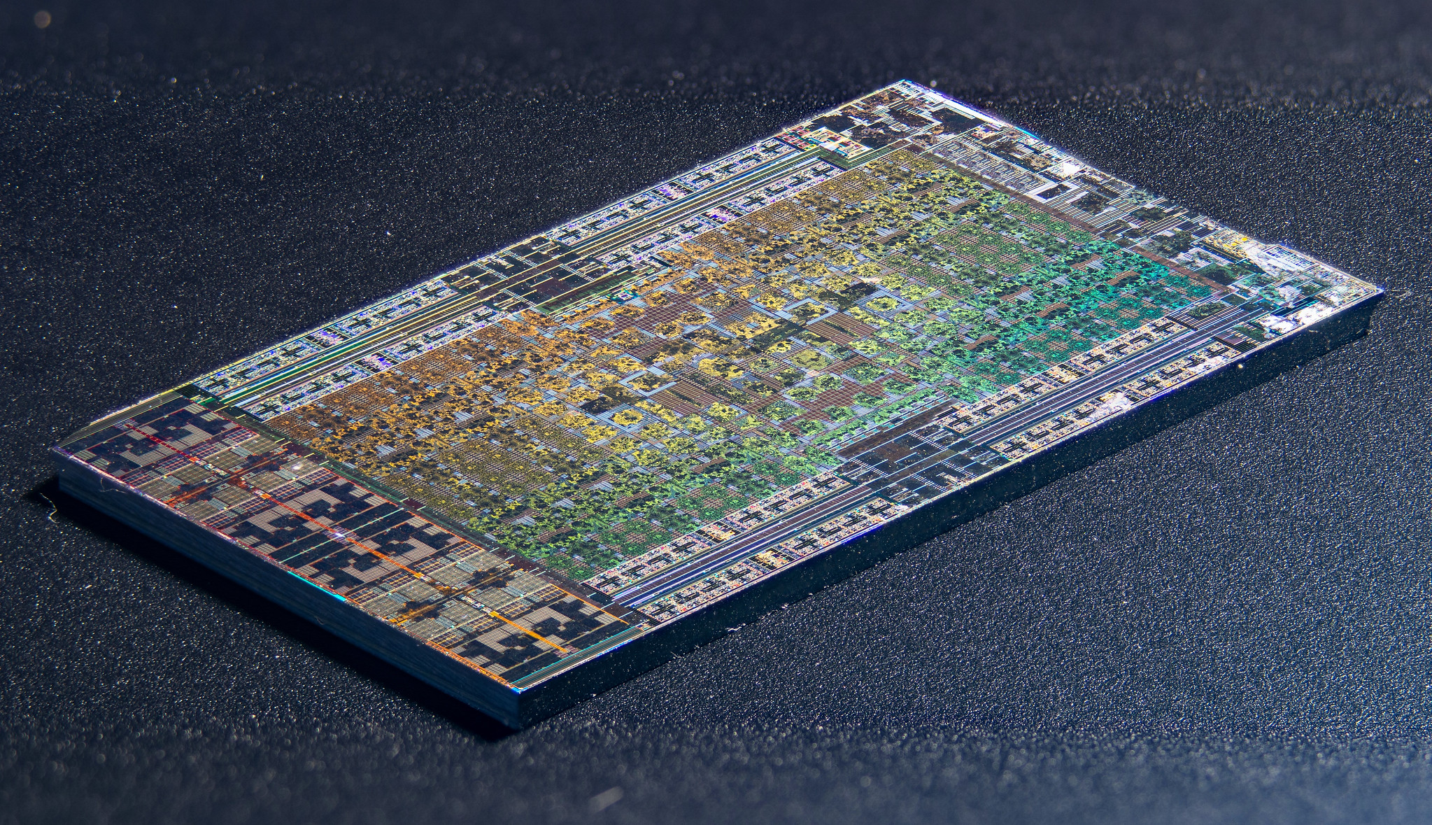
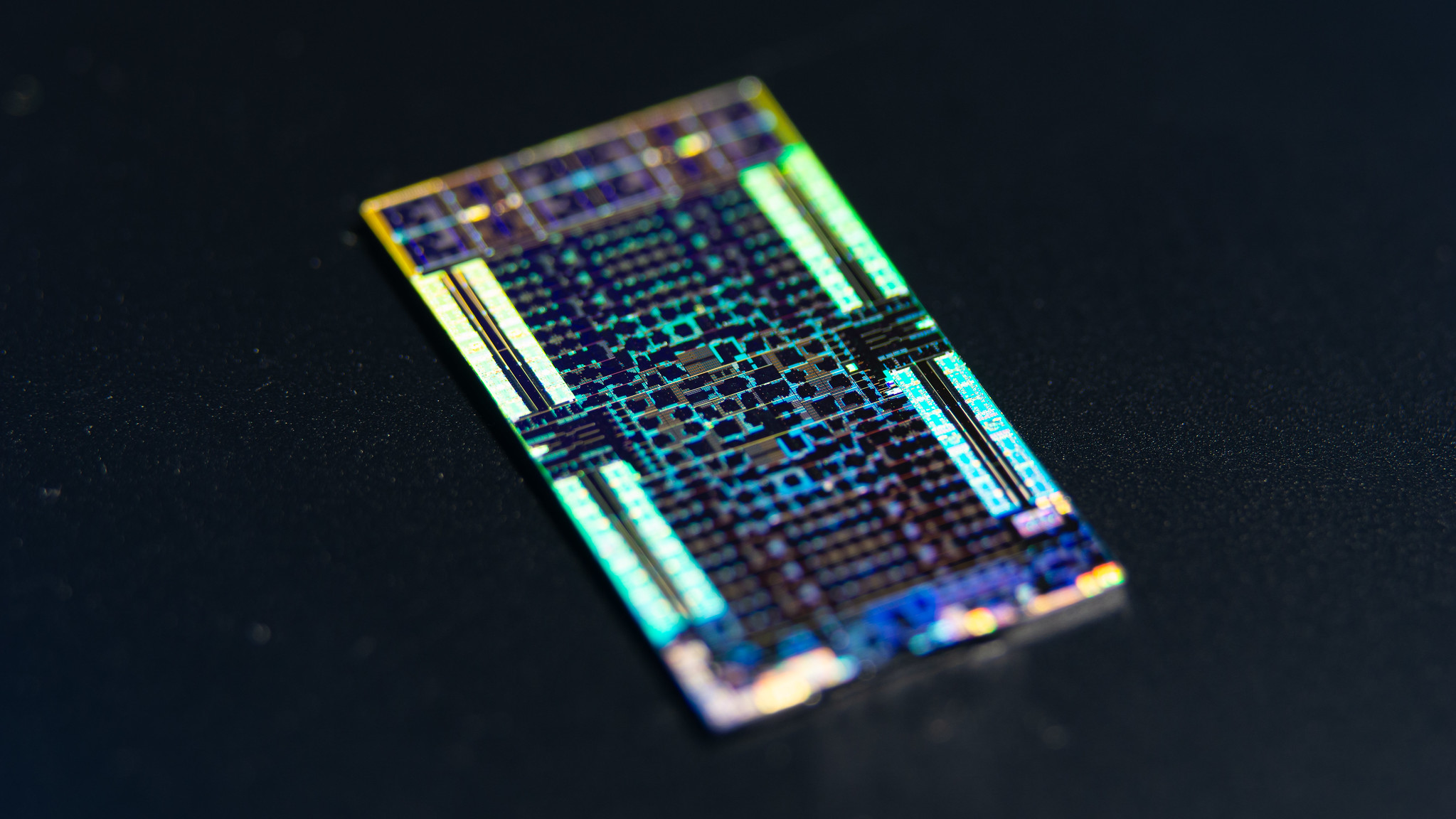
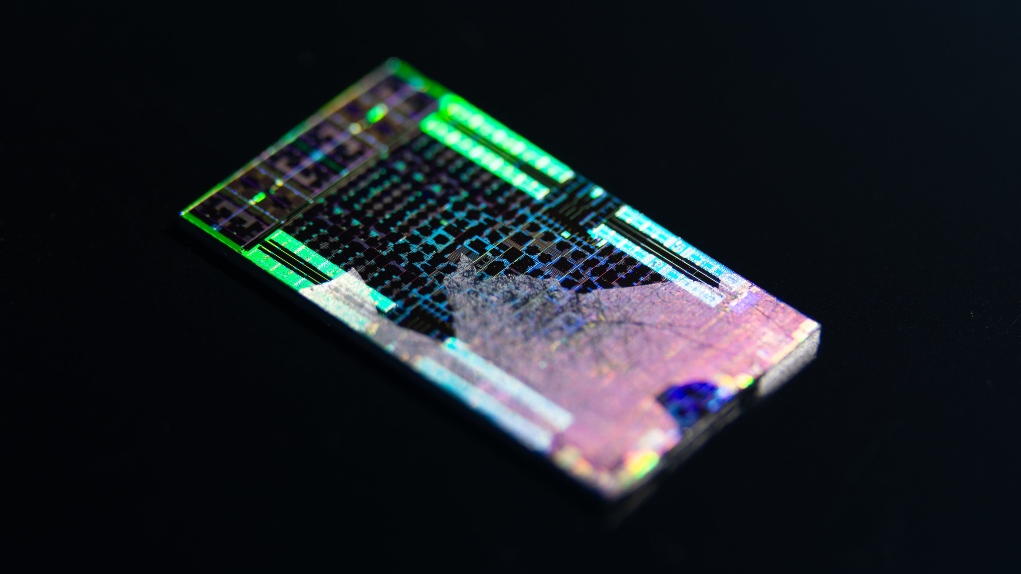
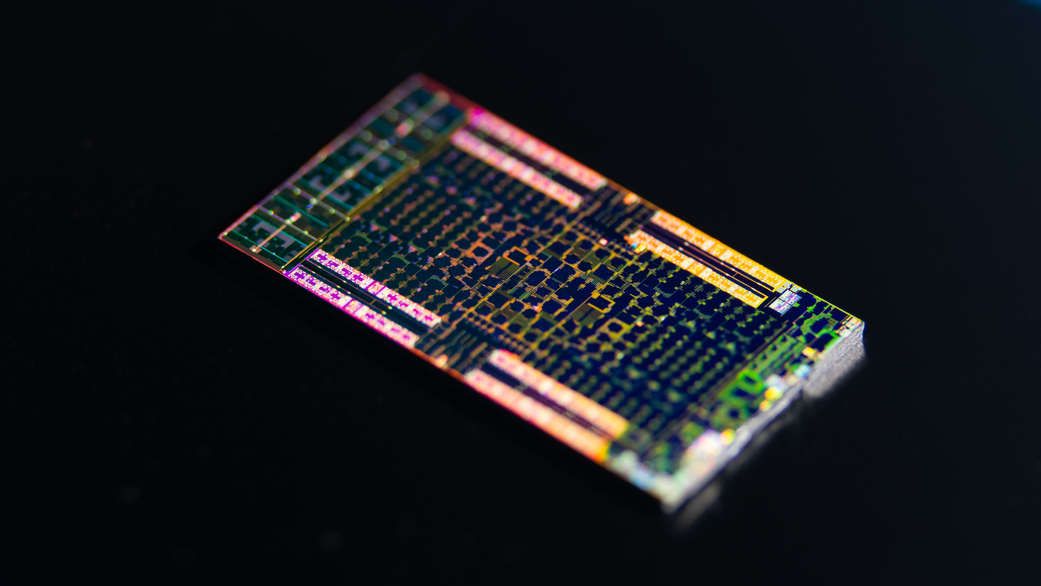
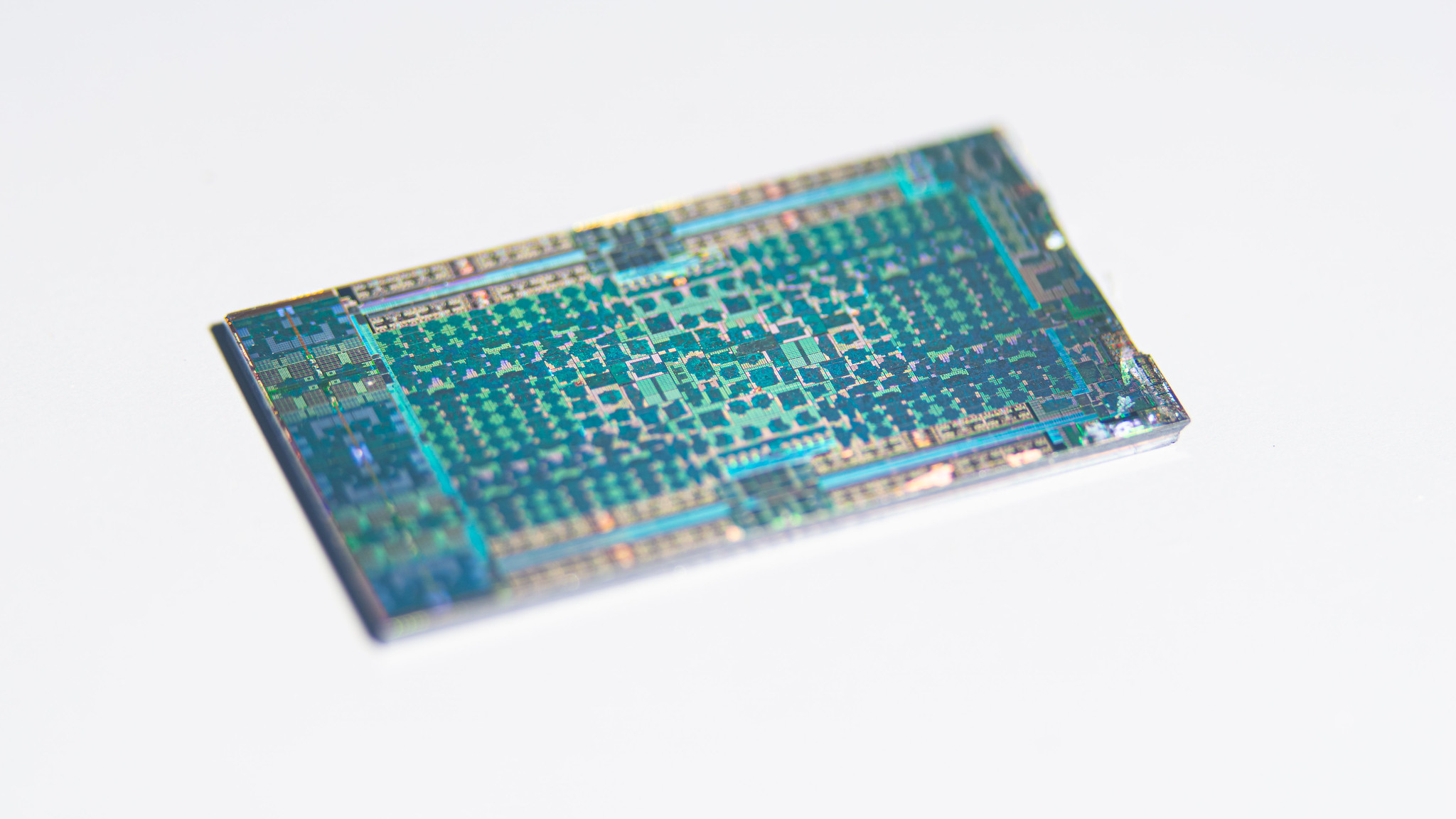
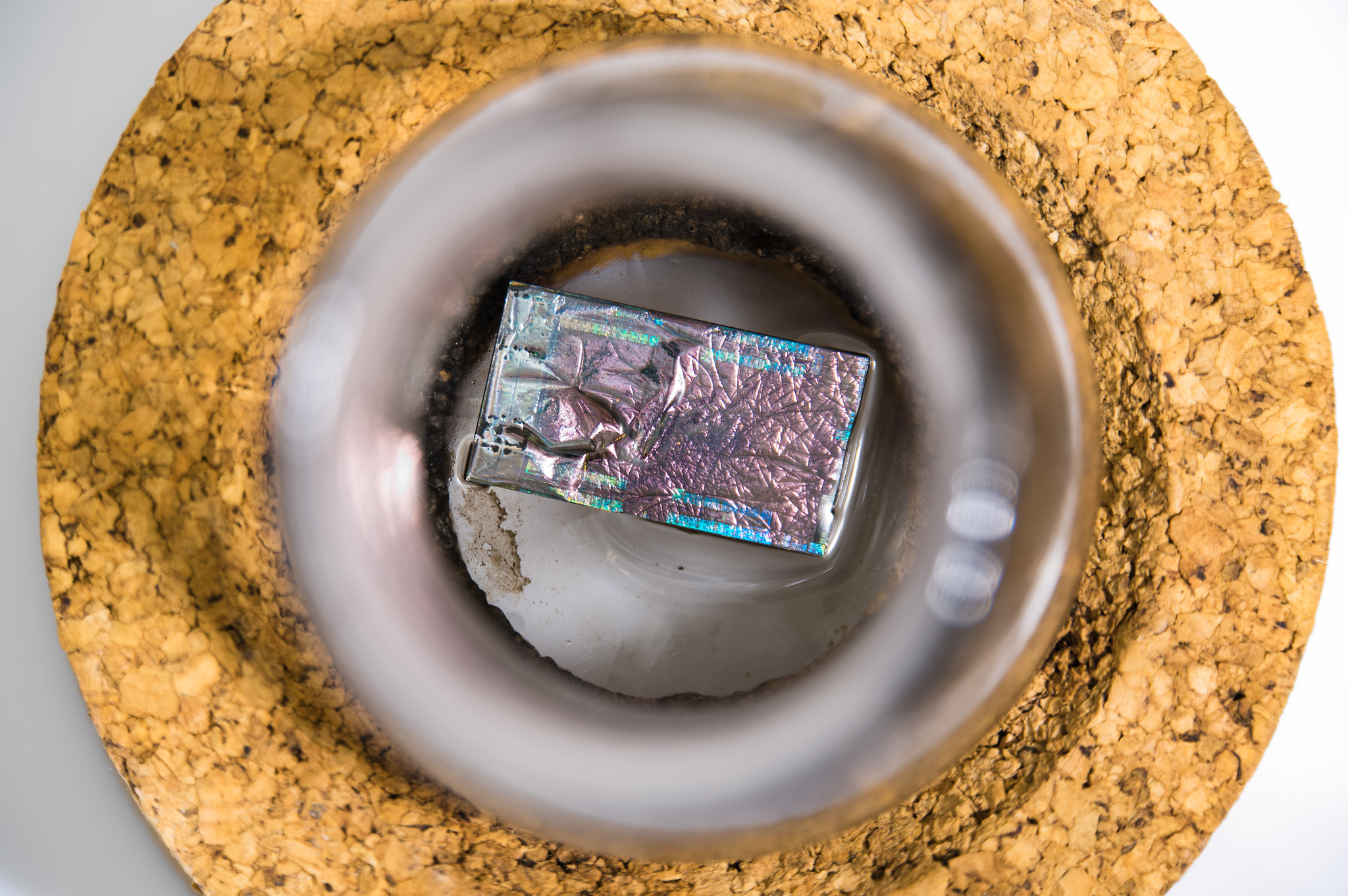
The die shots, which you can see in the gallery above, show how AMD laid out the billions of transistors across the entire chip. The GPU cores sit in the middle, split inside multiple CUs to form an integrated graphics engine. Beside them reside the aforementioned Zen 2 cores, followed by the silicon dedicated to I/O.
There is a clear indication of AMD's Infinity Fabric, which connects the entire chip, and L2 cache. The GDDR6X memory controller and PHY (physical layer) interface can be seen on the edge of the SoC, which is where the data enters and exits the processor. Looking closely, you can see the L3 cache there as well. You can also see the remaining images in the Fritzchens Fritz Flickr folder.
If you recall, this exact chip is the heart of the AMD 4700S desktop kit. However, it is slightly different due to the disabled graphics. Presumably, all of the chips that didn't reach full functionality have been repurposed for this desktop kit, meaning that the manufacturing process was the most difficult for the RDNA 2 graphics.
Stay On the Cutting Edge: Get the Tom's Hardware Newsletter
Get Tom's Hardware's best news and in-depth reviews, straight to your inbox.