AMD Files Patent for big.LITTLE-esque Hybrid Computing Technique
Big performance, low power
Get Tom's Hardware's best news and in-depth reviews, straight to your inbox.
You are now subscribed
Your newsletter sign-up was successful

As spotted by patent sleuth @Underfox3, AMD has field a patent for a technique that speeds the transfer of threads between high-performance cores and smaller low-performance cores in a big.LITTLE-esque hybrid computing architecture. As with all patent filings, this doesn't assure that AMD will bring a hybrid computing device to market, but it certainly shows the company is busy researching hybrid architectures.
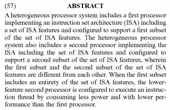
The patent outlines a new instruction set subset implementation for low power operation. AMD's patent describes an implementation that allows for one subset of instructions to execute on larger full-featured processing cores optimized for higher performance, while a second subset of instructions run on smaller simplified cores designed for power efficiency. The patent outlines a method for the cores to use a shared memory location to speed the transfer of threads, based upon certain variables, between the two types of cores.
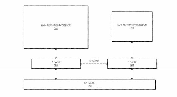
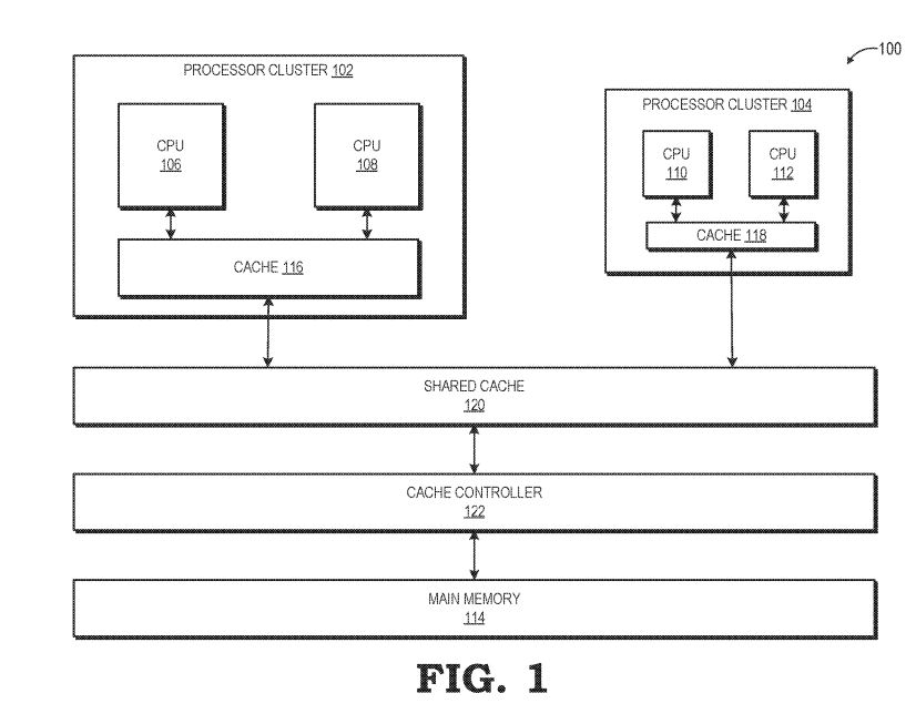
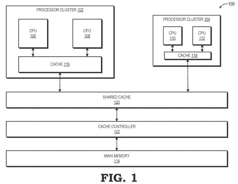
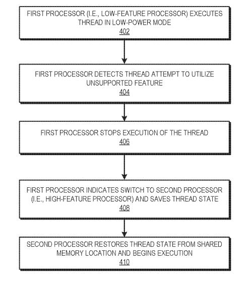
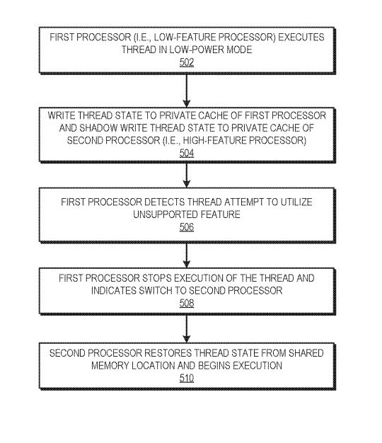
In practice, the big cores would execute heavy performance-sensitive workloads, while the smaller cores would execute light tasks. When a core isn't busy, it could be shut off, thus improving power consumption further.
Article continues belowIntel has already forged ahead with a hybrid design with its Lakefield chips (half-heartedly branded as Big-Bigger), but unlocking maximum efficiency requires the operating system and applications to be aware of the architecture so they can target threads to the correct cores. There's already plenty of work underway to support that technique.
The method described in AMD's patent appears to allow the processor to independently sort out which type of thread should run on each cluster based on the instructions supported by the cores within. The threads could also shift between the cores based on utilization. For example, if the large core is underutilized, the processor would shift the thread to the small core (provided it supports the instructions). If the small core is over-utilized, the thread would shift to the larger core (again, provided it supports the instructions).
The approach appears to reduce or negate the need for OS intervention for some types of thread movements. The patent also explains an example wherein the clusters of cores could be CPUs, GPUs, or DSPs, meaning there's a dizzying array of possible combinations.
Intel uses multiple stacked dies that it ties together with its Foveros 3D stacking die-to-die interface, but that type of advanced packaging tech isn't necessarily required for a hybrid design. If AMD releases a hybrid computing design, it could come as one large die or an MCM design that leverages many of the fundamental concepts behind its existing architectures, among other possibilities.
Get Tom's Hardware's best news and in-depth reviews, straight to your inbox.
However, as with all patents, AMD's filing doesn't guarantee that we will see new products based on the technique. Underfox also cautions that the patent is still in the adjustment phase, so it is subject to change. Regardless, the filing certainly shows that AMD is actively researching its own type of hybrid implementations.

Paul Alcorn is the Editor-in-Chief for Tom's Hardware US. He also writes news and reviews on CPUs, storage, and enterprise hardware.
-
jimmysmitty ReplyNightHawkRMX said:Is this comparable to what ARM and Intel now do?
Similar idea. No idea on the implementation. Intels Forevos is pretty advanced (die stacking) so I would think AMD would be looking for a similar technique. -
alextheblue Reply
Intel's current implementation requires ISA parity though... which harms the performance of the larger cores.jimmysmitty said:Similar idea. No idea on the implementation. Intels Forevos is pretty advanced (die stacking) so I would think AMD would be looking for a similar technique. -
TerryLaze Reply
It's foveros (the frightening one) you barbar. :pjimmysmitty said:Similar idea. No idea on the implementation. Intels Forevos is pretty advanced (die stacking) so I would think AMD would be looking for a similar technique.
Also do you really need stacking for big.little,you can have them seperate just like any CCX, or not? -
PCWarrior I look forward to the AMD fbs claiming that this is AMD's super-duper innovation, done for the first time ever by AMD and that everyone else is copying AMD. Like with the MCM/chiplet approach which was previously done by Intel 10 times: Intel Pentium Pro, Pentium D Presler, Xeon Dempsey, Xeon Clovertown, Core 2 Quad (Kentsfield, Penryn-QC and Yorkfield), Clarkdale, Arrandale, and Haswell-H. And when Intel decided to use MCM again for Kabylake G, Lakefield and Cooperlake it was supposedly a case of Intel copying AMD (disregarding the long history of Intel using MCM). I still remember like yesterday when AMD and their fbs were fighting MCM calling Intel that they are stitching dies together. And when Intel dared to say the same about Ryzen MCM (in an internal presentation mind you to highlight the performance benefits of monolithic dies) they got offended and didn't stop brigning up how supposedly now Intel is gluing dies with Cooper lake and Lakefield. This level of irony and hypocrisy never ceases to amaze me.Reply -
oGudNite As spotted by patent sleuth @Underfox3, AMD has field a patent for a technique... I believe you word correction might have made an errorReply -
digitalgriffin ReplyPCWarrior said:I look forward to the AMD fbs claiming that this is AMD's super-duper innovation, done for the first time ever by AMD and that everyone else is copying AMD. Like with the MCM/chiplet approach which was previously done by Intel 10 times: Intel Pentium Pro, Pentium D Presler, Xeon Dempsey, Xeon Clovertown, Core 2 Quad (Kentsfield, Penryn-QC and Yorkfield), Clarkdale, Arrandale, and Haswell-H. And when Intel decided to use MCM again for Kabylake G, Lakefield and Cooperlake it was supposedly a case of Intel copying AMD (disregarding the long history of Intel using MCM). I still remember like yesterday when AMD and their fbs were fighting MCM calling Intel that they are stitching dies together. And when Intel dared to say the same about Ryzen MCM (in an internal presentation mind you to highlight the performance benefits of monolithic dies) they got offended and didn't stop brigning up how supposedly now Intel is gluing dies with Cooper lake and Lakefield. This level of irony and hypocrisy never ceases to amaze me.
Theres a huge difference between mcm packages and the use of interposers which AMD was the first to use. They aren't even in the same ball park.
Then intel attacked AMD claiming they were gluing chips together when the 3000 series was introduced.
Intel has their own technology in Feveros now. Intel claims it's superior. However rumors are the ring bus coherency between chip caches is a nightmare. This is what was a big issue with ccx on the 3000 series. But supposedly mostly solved with 4000 series. And I think I have an idea how they did it.
The big little design is an interesting layout in feveros. The little cores dont directly align with the big cores over them. So straight interconnect stacking of big-small isn't a thing. It has to be some hybrid ring bus design. -
JamesSneed This whole hybrid computing is pointless unless you are severely TDP constrained think tables or smaller. You are simply one full node of process improvement away from having all large cores . The SoC fragmentation this causes is going to be a complete pain especially if everyone does there own hybrid computing approach. I have no doubt Microsoft would screw up the kernel trying to deal with these differences. I'm not a fan of this at all. For example we will see Intel's Tiger Lake get dominated by AMD's next gen APU's(Zen3/RDNA2) later in 2021 because of the better process and all large cores.Reply -
BillM1 ReplyAdmin said:A recently filed AMD patent suggests the company is researching a big.LITTLE-esque hybrid architecture that employs big, fast cores paired with smaller cores that improve power efficiency.
AMD Submits Patent for big.LITTLE-esque Hybrid Computing Implementation : Read more
I would be surprised if this could stand up to any review. Why, for decades, PCB systems have had multiple CPUs spread across the system/board to perform processing. Their have even been CPU/GPU and GPU/GPU processing setups to help offload processing to other components. Too little shown but it would be interesting if/when Intel determines they need to challenges this... -
Chung Leong ReplyNightHawkRMX said:Is this comparable to what ARM and Intel now do?
The key innovation here is the use of the instruction stream to trigger transitions. I think the technique is mainly designed for servers, where you can't rely on external signals to infer which core is the proper one at a given moment. On a phone or a laptop, there're foreground and background threads. There're threads that draw to the screen and those that don't. There're also different power conditions. Based on these variables, you can build an effective heuristic. On a server, you have none of these.