Alleged AMD Phoenix 2 Laptop CPU Die Shots Hit the Web
The next instance of AMD's Phoenix is apparently catering to lower-end laptops as well.

Get Tom's Hardware's best news and in-depth reviews, straight to your inbox.
You are now subscribed
Your newsletter sign-up was successful
Considering the buzz around AI and the reception surrounding its 7040-series Phoenix APUs, it was only a matter of time before we'd see new products from AMD leveraging the latest AI processing core. Once again, it seems that AMD elected to manufacture the highest-performing and higher Average Selling Price (ASP) products first. But AMD was bound to trickle down its Zen 4 + RDNA 3 + XDNA AI Phoenix processing package to additional, smaller chips. And if leaked photos are anything to go by, AMD's next chip in the Phoenix line is substantially lower in performance compared to the 7040U the company announced just two months ago.
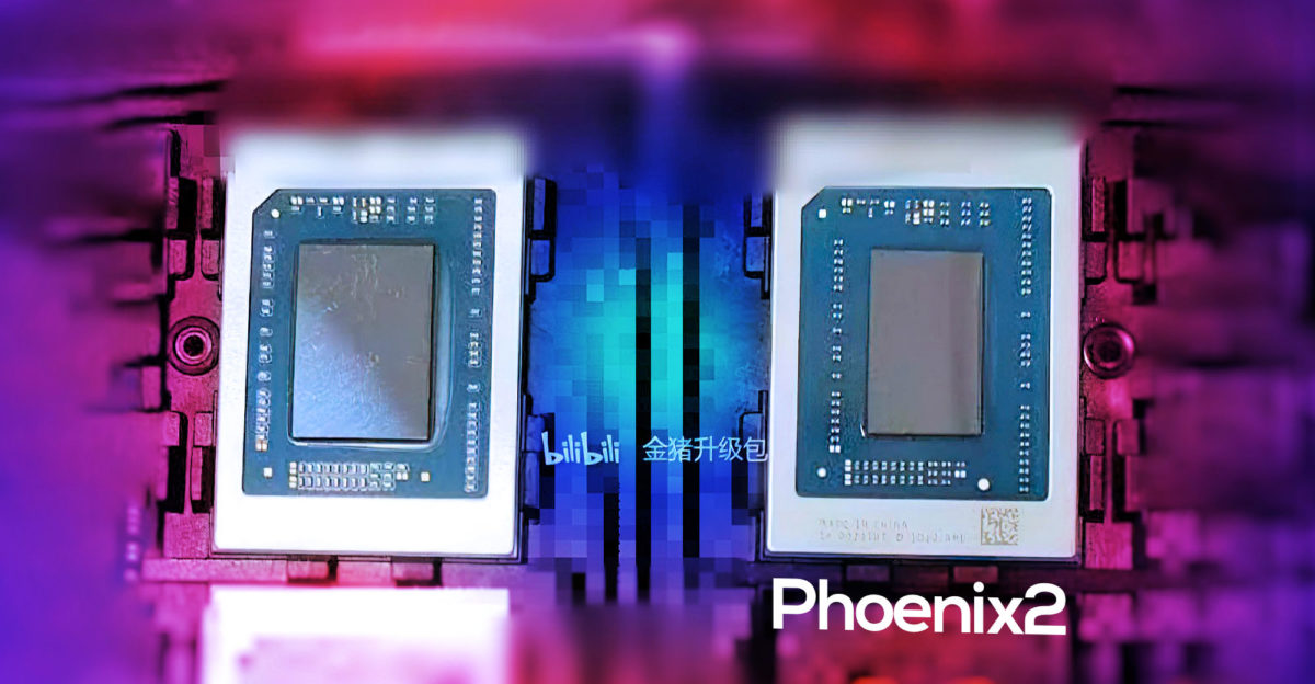
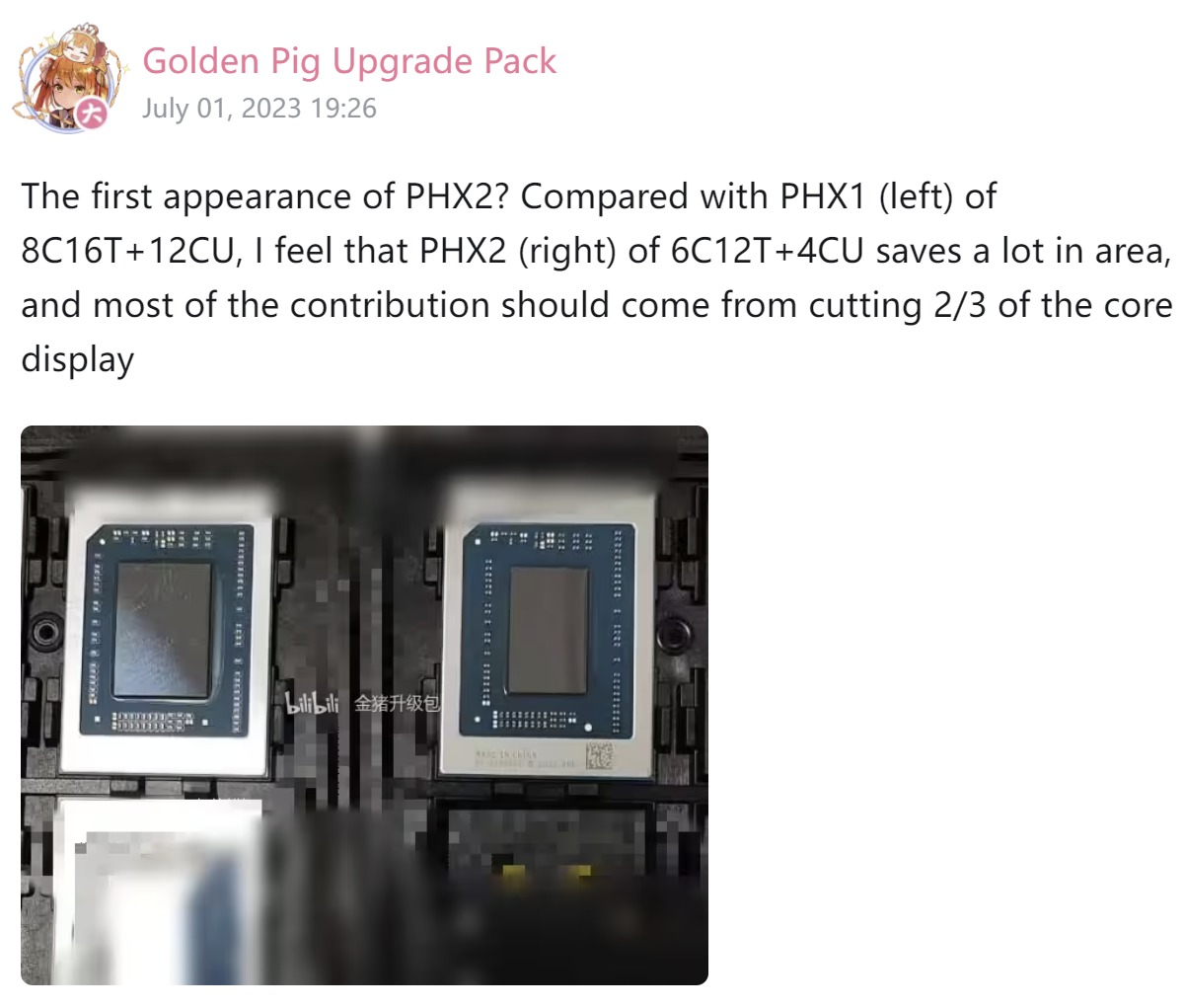
The Phoenix 2 will allegedly be a smaller chip than the original while bringing the same feature set to a lower price point. However, that lower price point can only be achieved one way without cutting into the chips' features and design, and that's by reducing the silicon area dedicated to processing resources. That move sees Phoenix 2 shed around 23% of its silicon area, taking the die area from 178 mm2 to just 137 mm2.

Unfortunately, these cuts will likely come at a significant performance penalty. While Phoenix 1 could support up to 8 cores / 16 threads (Zen 4) and 8-12 CUs, it seems that Phoenix 2 will max out at 6 cores. An even bigger cut is expected regarding the GPU, with only 4 CUs compared to the maximum 12 available to Phoenix.
Article continues belowThe die area savings will definitely impact performance by more than the 23% area saved; there's no way around that when you're cutting your CPU resources by 25% and your GPU resources by a whopping 66%. Phoenix 2 will likely be marketed under the Ryzen 5 and Ryzen 3 brands rather than the Ryzen 7, with model names like "Ryzen 5 7540U" and "Ryzen 3 7340U".
Looking elsewhere on the internet for information, sleuth Nemez (@GPUsAreMagic) took to Twitter to try and shed some light on what exactly makes up a Zen 4 CPU. Using patience, CPU design knowledge, and a Thermopylae-like sense of duty, Nemez managed to more or less circumscribe Zen 4's hardware design down to its essential elements: L1 and L2 cache repositories (which keep data close to the CPU's execution units, where they can more quickly be fetched); schedulers (which try to keep the CPU free of bottlenecks and stalls where information isn't where it's supposed to be at the moment it's needed); branch predictors...
Alrighty #silicongangTook longer since I'm busy with life, but finally - my interpretation of the Zen 4 core floorplan.The BPU just keeps getting bigger + an interesting FPU re-arrangement from Zen 3.One day I will count the TSVs too 🙃Photo credit: @FritzchensFritz 🩷 pic.twitter.com/0U59YAOOvaJune 26, 2023
The die shots also showcase how much die area is dedicated to things "other than the CPU cores." It's sometimes hard to understand how much logic goes into a modern processor, especially when marketing departments try to keep things as "simple" as possible. There are only mentions of either cores, threading, or (god forbid we get back there again) frequency. But none of those parts work without the rest of the "supporting" (but still essential) hardware.
So it seems AMD is readying a smaller version of its Phoenix CPUs, bringing its XDNA AI processing unit to lower-tier processors. AMD also had little choice but to cut on Phoenix 2's processing resources to shave area (and thus cost).
Get Tom's Hardware's best news and in-depth reviews, straight to your inbox.

Francisco Pires is a freelance news writer for Tom's Hardware with a soft side for quantum computing.
-
Reply
Phoenix 2 will likely be marketed under the Ryzen 5 and Ryzen 3 brands rather than the Ryzen 7, with model names like "Ryzen 5 7540U" and "Ryzen 3 7340U".
Slight typo. It's Ryzen 3 7440U, and not 73.
Also, these SKUs would also be using two types of cores, ZEN 4 and ZEN 4c. Either a full flat "Phoenix 2" die, or a cut-down Phoenix 1 die. So that's 2 high+4 low core config, or 8 high-clock cores binned down to '2 high-clock + 4 low-clock' cores (since Zen 4c is just a down-clocked version of Zen 4).
Basically these are dual-sourced chips.
The Zen 4C core is a cut-down version of Zen 4, which is downclocked, making it possible for the APU to bin down from 8 high-clock cores to 2 high-clock and 4 low-clock cores. This is most probably AMD's version of the "hybrid" strategy that was previously revealed.
Zen 4 and Zen 4C cores are mostly the same design in my opinion, but the latter is optimized for "density" and features a lower cache. -
TechyIT223 Why are they using 2 as a suffix? so only two models come under the phoenix 2 lineup ?Reply