Gigabyte's RTX 4090 has Traces of NVLink
Is Gigabyte repurposing 3090 circuit boards, or did it just get Nvidia's memo too late?

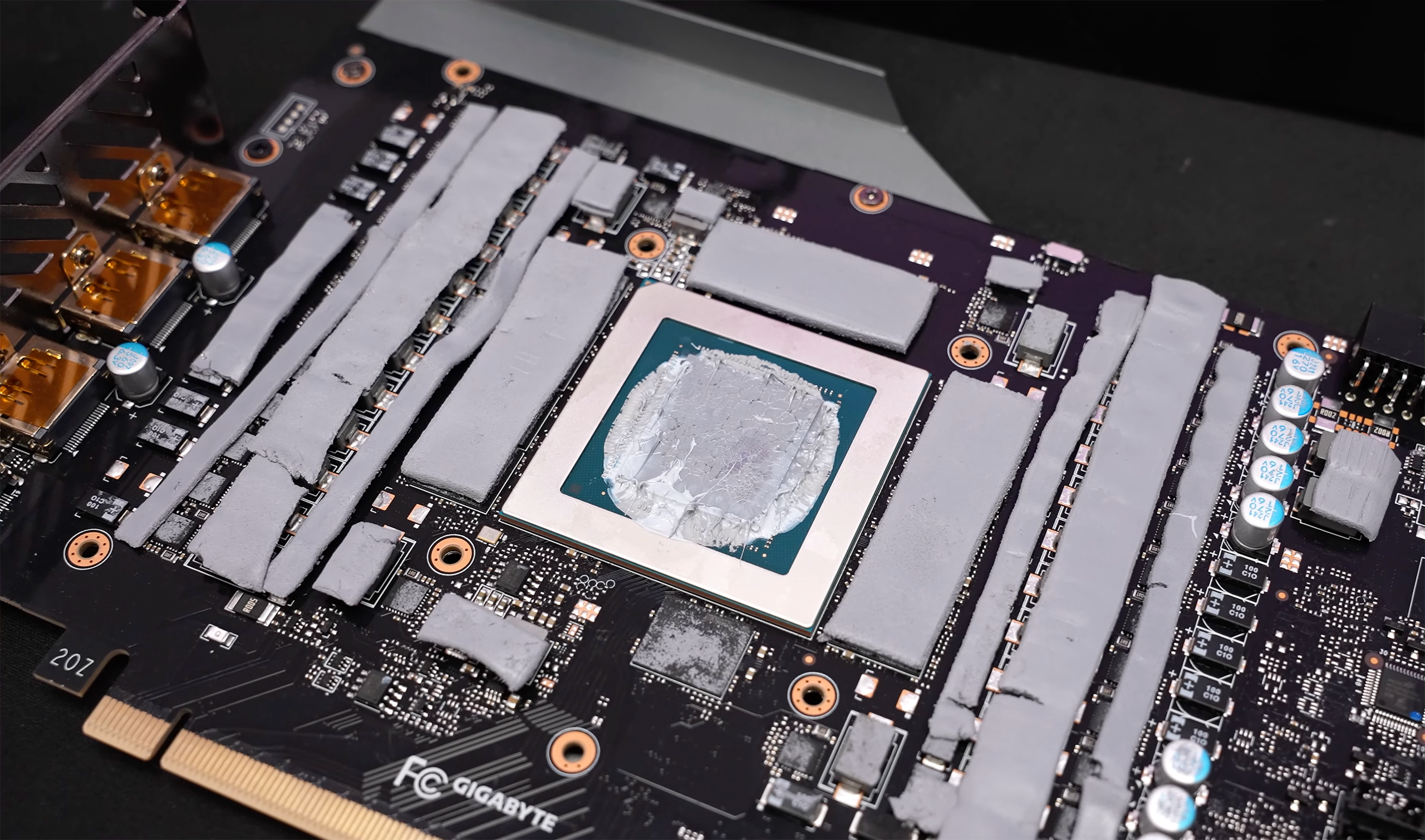
Nvidia's GeForce RTX 4090 graphics card may not support NVLink, but traces can be found on Gigabyte's Aorus Master GeForce RTX 4090 board.
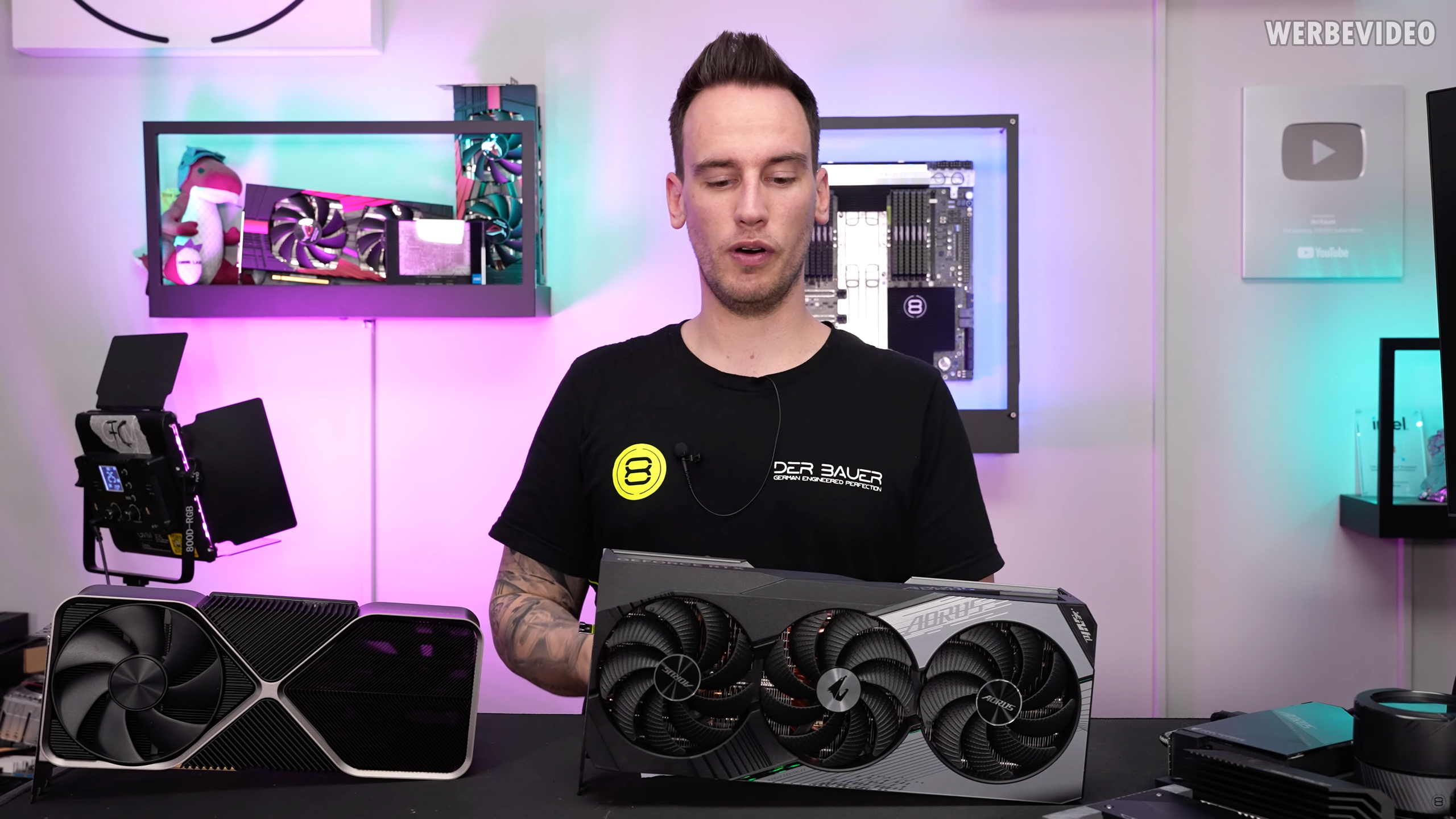
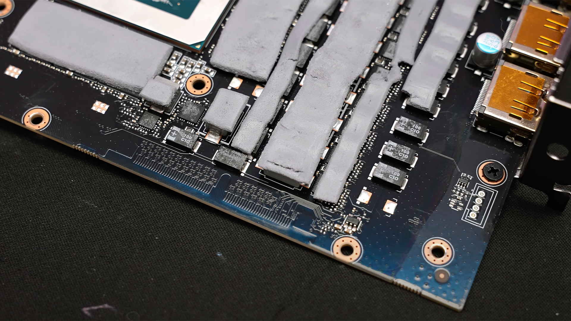
Legendary overclocker Roman 'der8auer' Hartung this week disassembled Gigabyte's Aorus Master GeForce RTX 4090 graphics card (one of the best graphics cards around) and found that its printed circuit board (PCB) had a place for NVLink contacts. There was no actual copper on the grid, but the fact that the company left such traces was intriguing.
Indeed, Nvidia officially said that its AD102 graphics processor did not support NVLink interconnect as it decided to use transistor budget and die space for other purposes. Thus, NVLink is gone from Ada Lovelace client GPUs — and other GeForce RTX 4090 boards we've seen so far did not have any traces of NVLink. In fact, our colleagues from VideoCardz even checked pictures of RTX 4090 PCBs from Asus, Colorful, MSI, Palit, and Zotac (published by TechPowerUp) and found no traces of NVLink.
There are a few possible reasons for why Gigabyte left NVLink pads on its GeForce RTX 4090 graphics card.
The AD102 graphics processor and the GA102 graphics processor are pin-to-pin compatible, so it's possible Gigabyte just re-used printed circuit board of its GeForce RTX 3090 Ti for its GeForce RTX 4090 to save on development costs (we cannot confirm this as we have not seen PCB design of Gigabyte's Aorus Master GeForce RTX 3090 Ti). The company might have a boatload of unused GeForce RTX 3090 Ti PCBs and throwing them away would be expensive, so re-using them makes sense.
Or perhaps Nvidia notified Gigabyte about the lack of NVLink in the AD102 GPU too late and Gigabyte decided not to reiterate its PCB design to ensure rapid time-to-market.
A few people might miss NVLink on GeForce RTX 4090, but it was actually surprising that the technology ever made it to client GPUs (in some Turing GPUs) at all.
Get Tom's Hardware's best news and in-depth reviews, straight to your inbox.
Nvidia's NVLink interconnect was originally designed to be a high-bandwidth (300 GB/s P2P over six lanes on Volta, 900 GB/s P2P over 18 lanes on Hopper) low-latency link between CPU and GPUs in systems used for high-performance computing (HPC) and data analytics. The technology was incorporated into IBM's Power 8 processors — but since modern CPUs from AMD and Intel do not support the interconnect, Nvidia can only use it as a multi-GPU interconnection.
NVLink wasn't really meant for client devices, but Nvidia incorporated such links into client GPUs to enable multi-GPU support mainly for professional applications (including graphics and HPC workloads) as well as for a few extreme gamers with very deep pockets.
With its AD102 GPU Nvidia decided that incorporating NVLink into a client GPU makes less sense than maximizing its performance by increasing its transistor budgets for computing. While a dual-GPU graphics subsystem consisting of two AD102-based RTX 6000 48GB professional graphics cards would have offered advantages to HPC and some graphics professionals (think 96GB of graphics memory), Nvidia still didn't think it made enough sense to add NVLinks to AD102.

Anton Shilov is a contributing writer at Tom’s Hardware. Over the past couple of decades, he has covered everything from CPUs and GPUs to supercomputers and from modern process technologies and latest fab tools to high-tech industry trends.

