Inside Intel's CPU Packaging Factory: From Wafer to Chip
Touring Intel's Malaysian facilities.
Get Tom's Hardware's best news and in-depth reviews, straight to your inbox.
You are now subscribed
Your newsletter sign-up was successful
Kulim Die Sort and Die Preparation (KMDSDP)
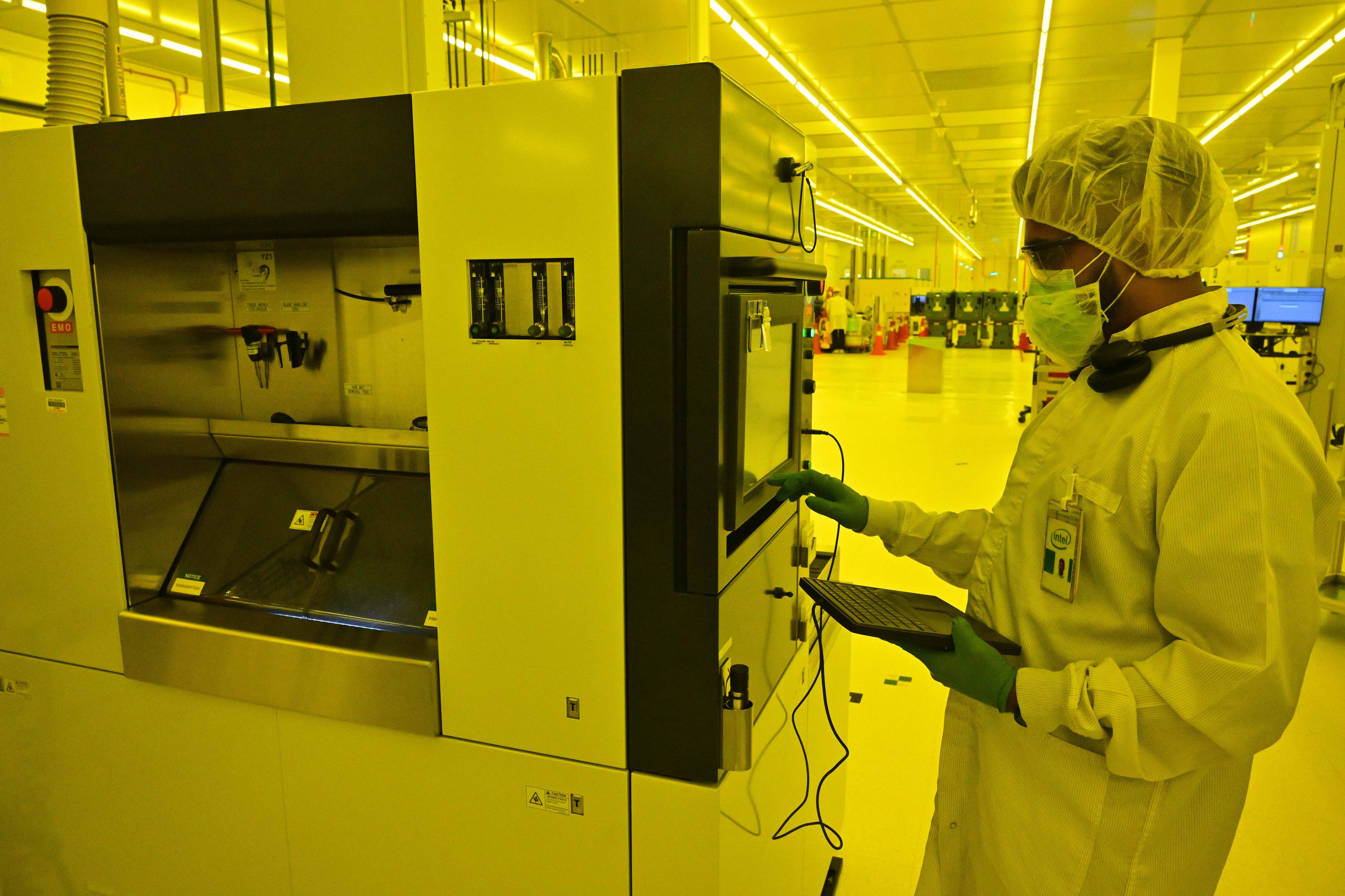
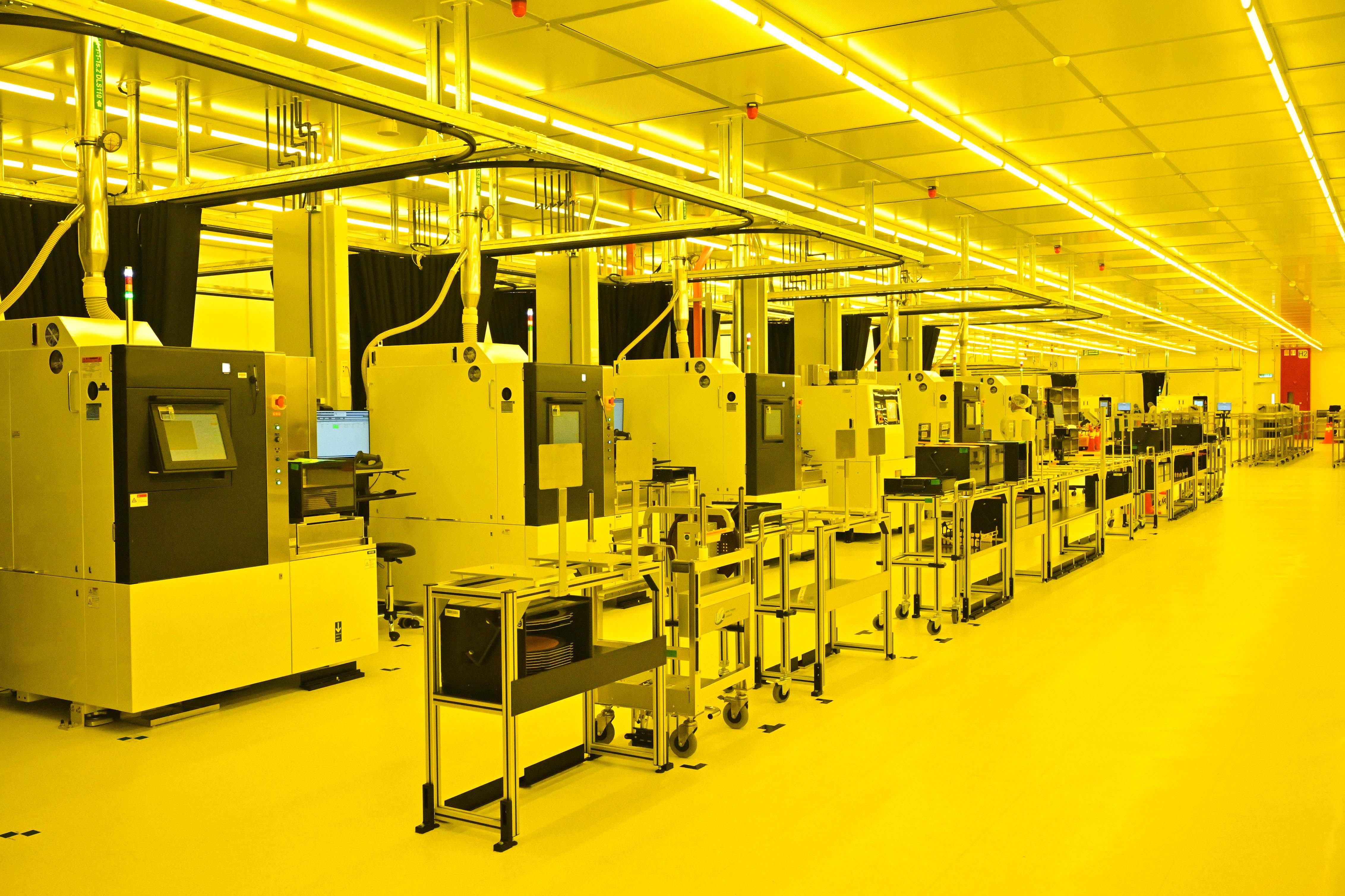
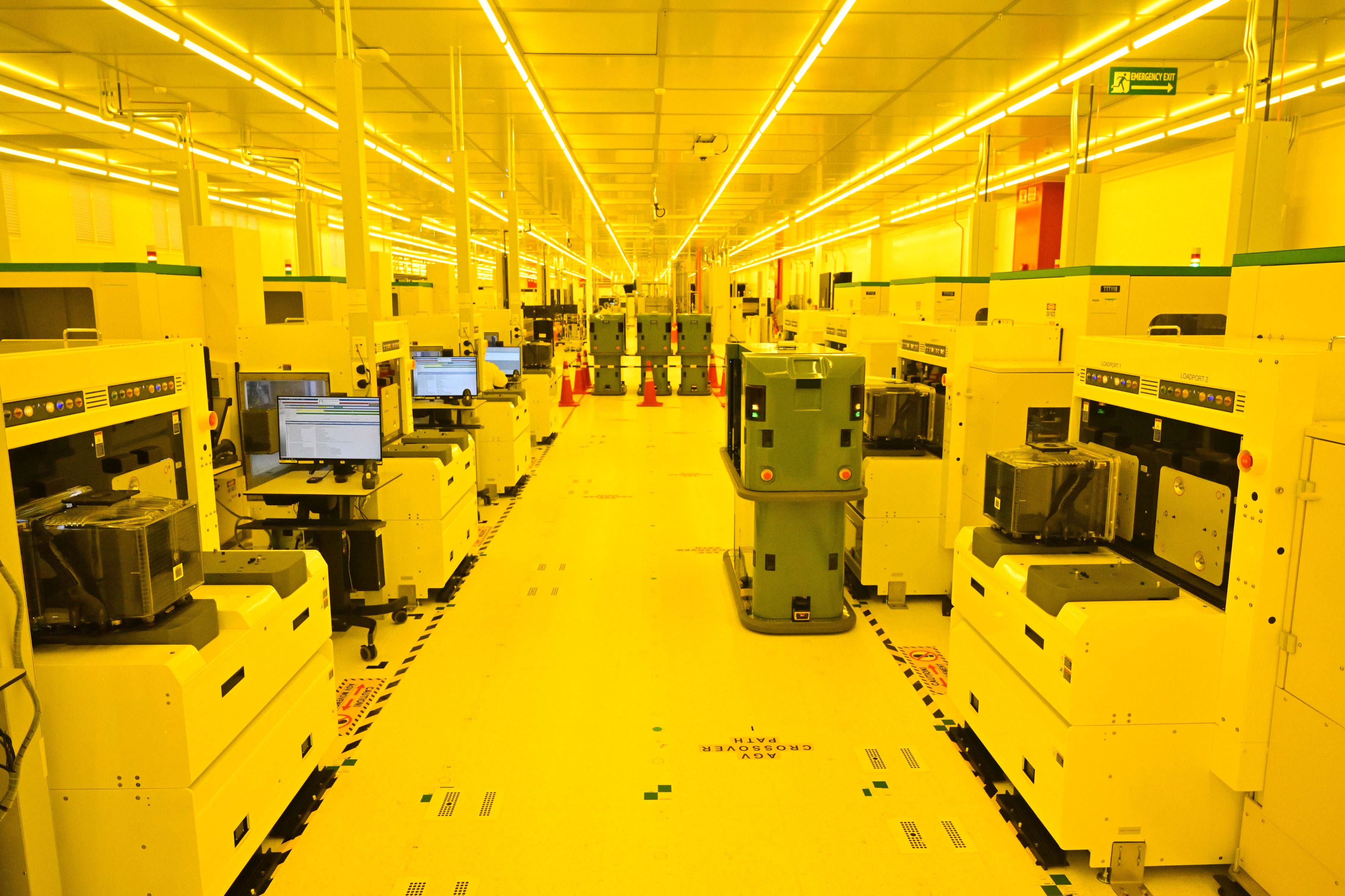
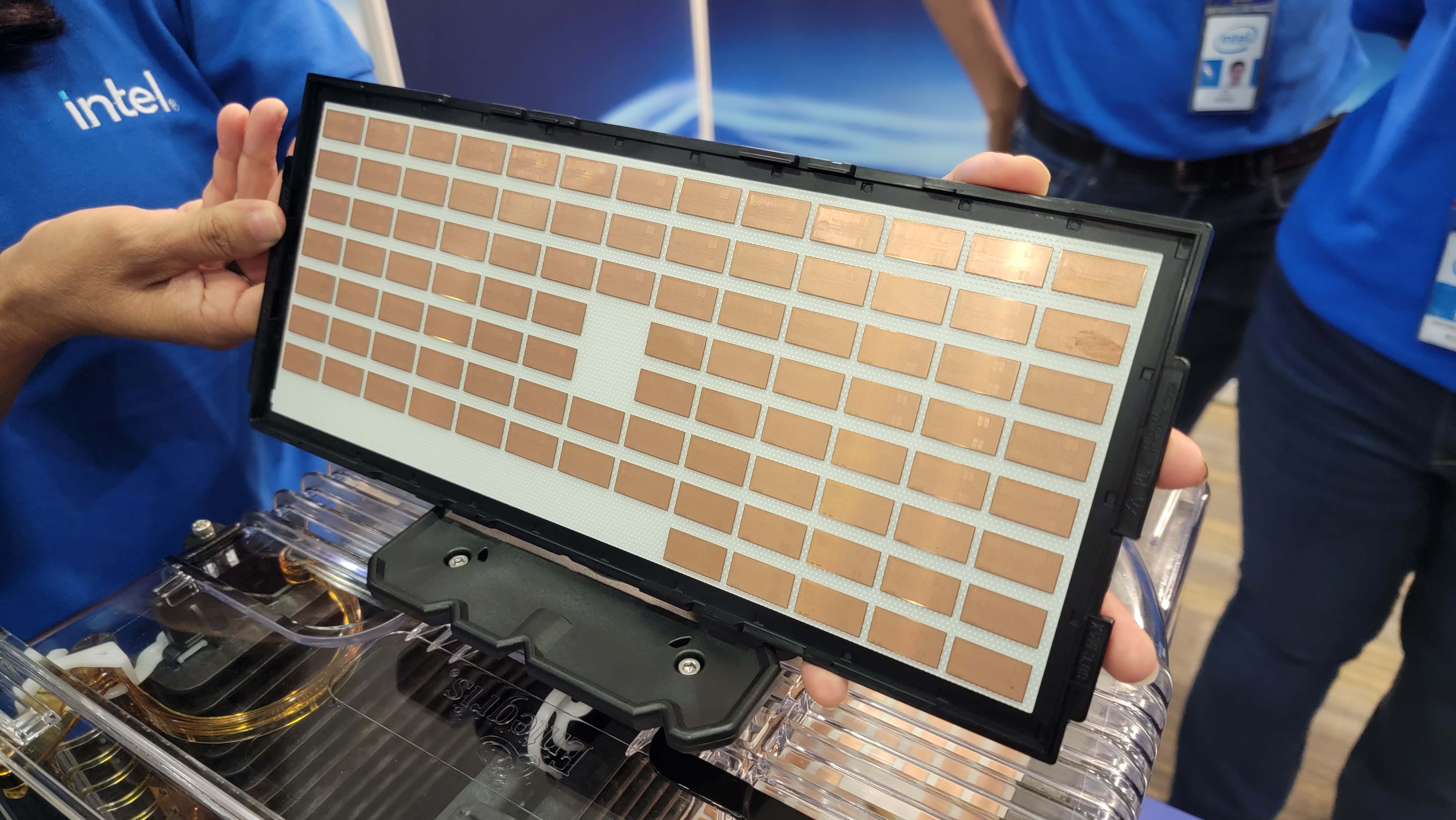
This is the only area of the tour that Intel didn't provide B-Roll footage for, which is understandable given that nearly all of the equipment used here is proprietary. You'll see plenty of interesting videos on the following pages.
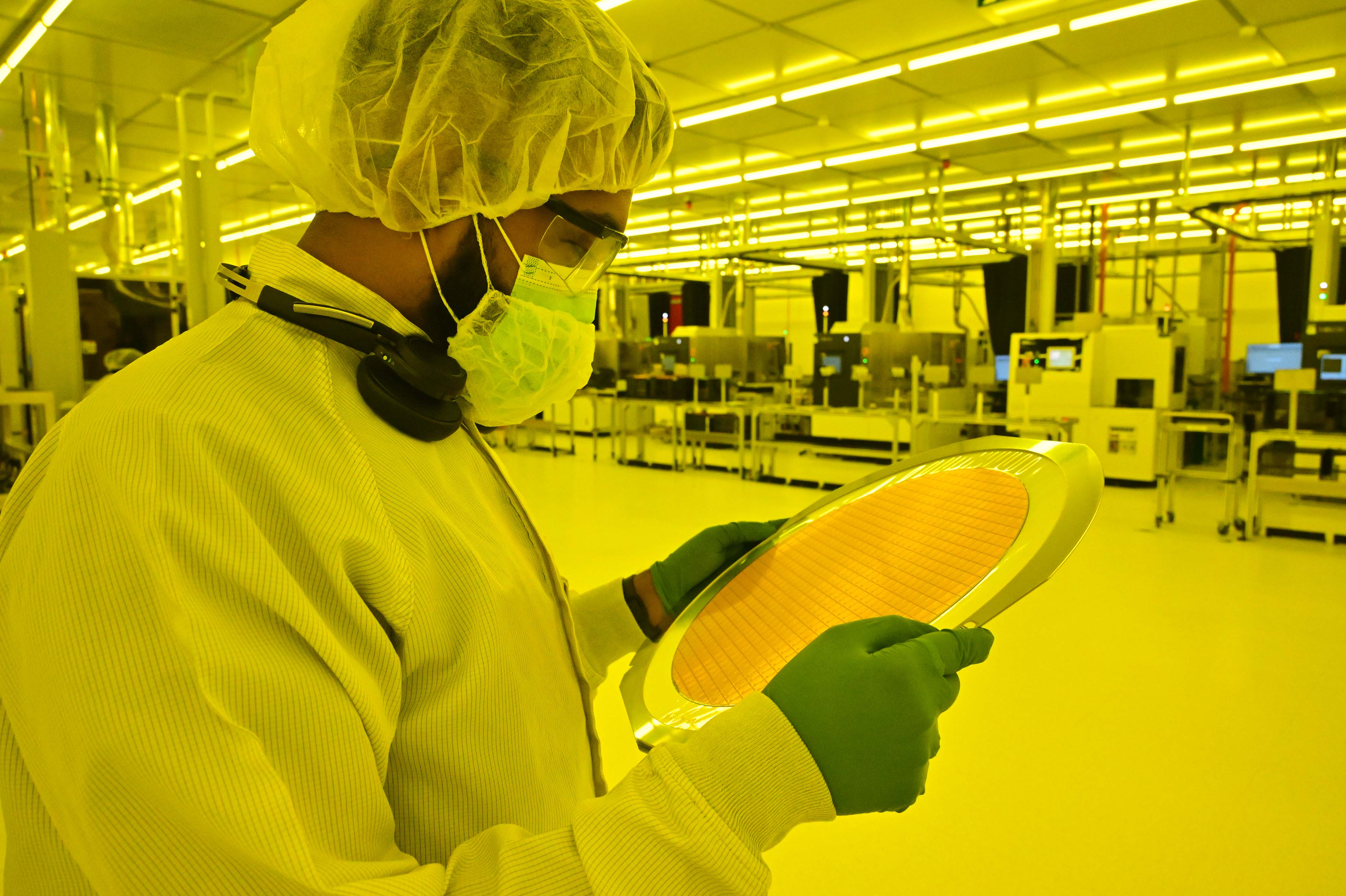
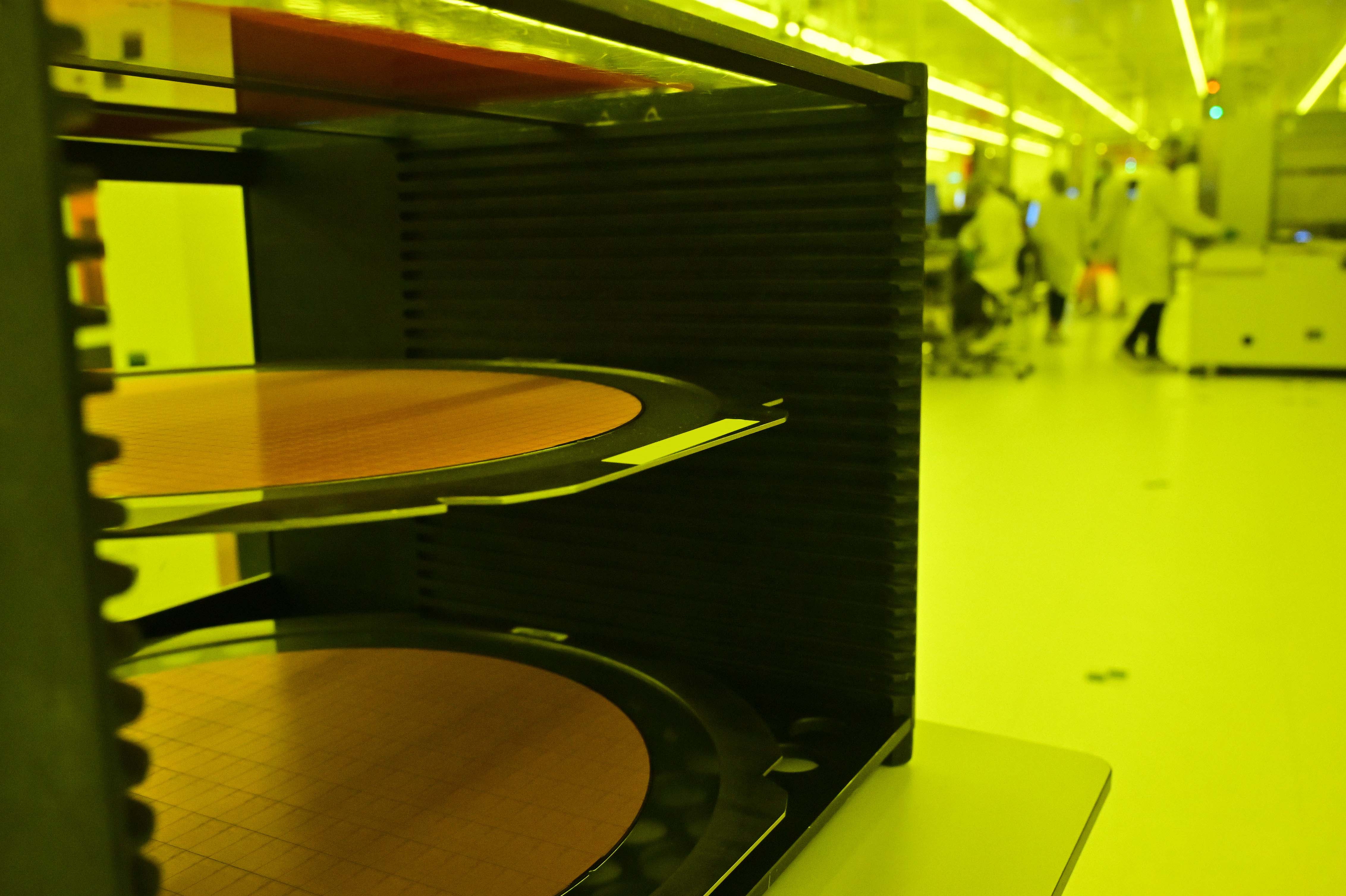
At the Kulim Die Sort and Die Preparation (KMDSDP) facility, the newly arrived 300mm wafers are placed onto a carrier frame with a sticky and flexible Mylar sheet in the middle that holds the wafer in place. Some dies, like those for mobile processors, require thinning first to reduce the Z-height of the wafer. The back of the wafer is first ground down, then it's flipped onto another mylar carrier frame for additional processing. This area is bathed in amber light because regular UV light degrades the Mylar backing, causing it to lose its adherent properties.
The wafer carriers are then placed into a front-opening universal pod (FOUP)-like device, a plastic carrier that holds multiple wafer carriers stacked vertically, and moved to a laser scribing machine that etches the wafers around the individual die to provide guidance for the sawing process.
After scribing, the FOUP is placed into a wafer-slicing machine with diamond-bladed circular saws that are watercooled by powerful waterjets that direct liquid onto the saw blades during the cutting process. Intel didn't include a picture of the internals of the slicing machine, but two saw blades can work at the same time on a single wafer, cutting the wafer into individual dies. The powerful water jets both cool the blade and remove particles, with the water spitting back and obscuring the viewport that allows the technician to monitor the process.
The sawing process, referred to as singulation, moves incredibly quickly given the micron-scale precision — the saws cut the wafers while only partially penetrating the super-thin mylar sheet beneath the wafer on the carrier frame, effectively only scratching it while cutting the wafer within microns of the functional logic units (transistors) on the dies.
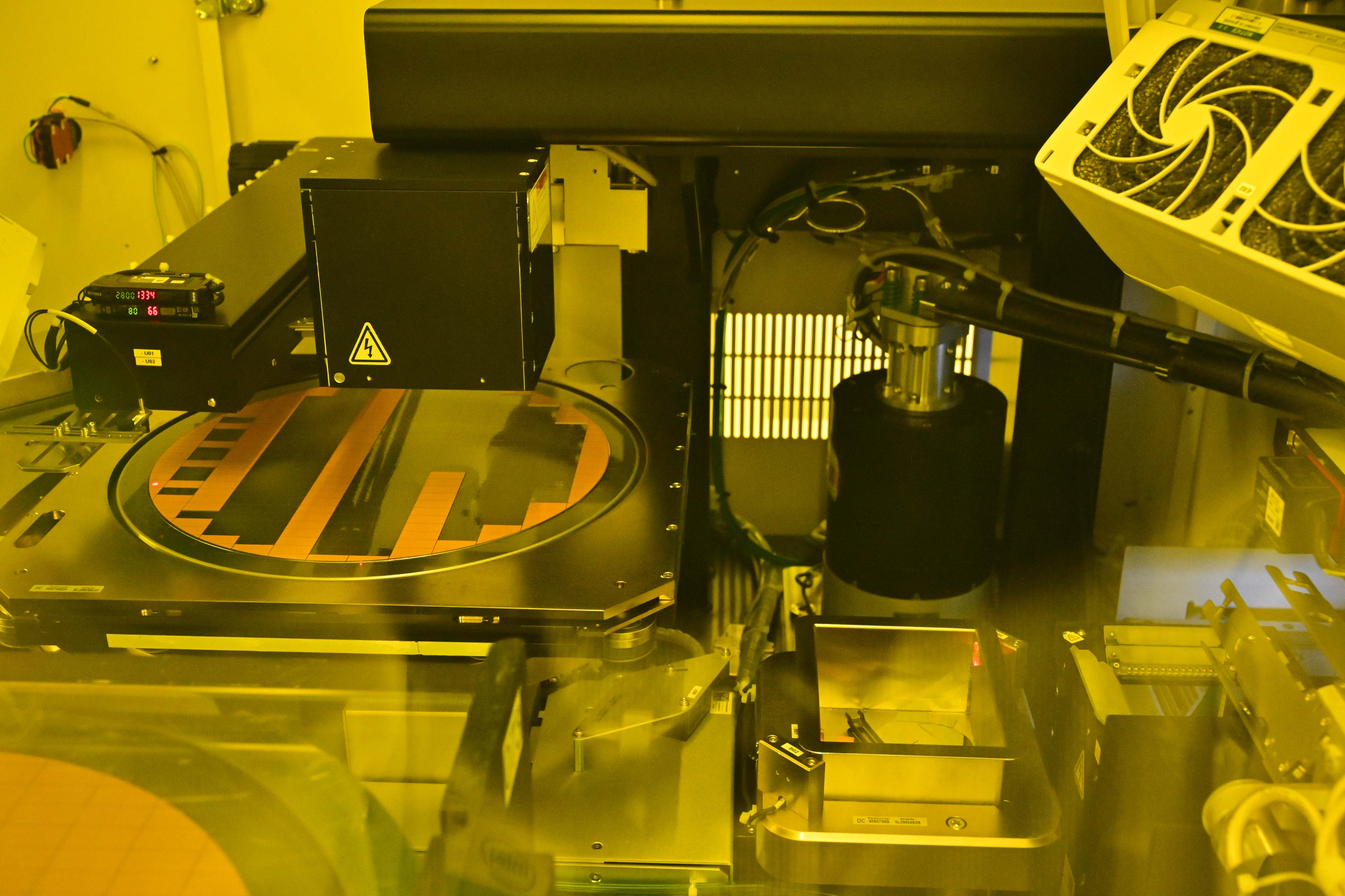
The carrier frame is then placed back into the FOUP and moved to the pick and place machine (fourth image in the above album). Here the mylar is exposed to UV light to reduce its adherence while pins push from underneath to free the die from the mylar. Simultaneously, a robotic arm grabs the individual die using vacuum suction and swings it across to a sticky die carrier frame (last image).
Again, this process moves at breakneck speed, with each die being lifted and swung to the carrier in a fraction of a second, speedily dismantling the wafer into separate dies. Known defective dies and the unused die around the periphery of the wafer are left in place on the carrier frame to be discarded.
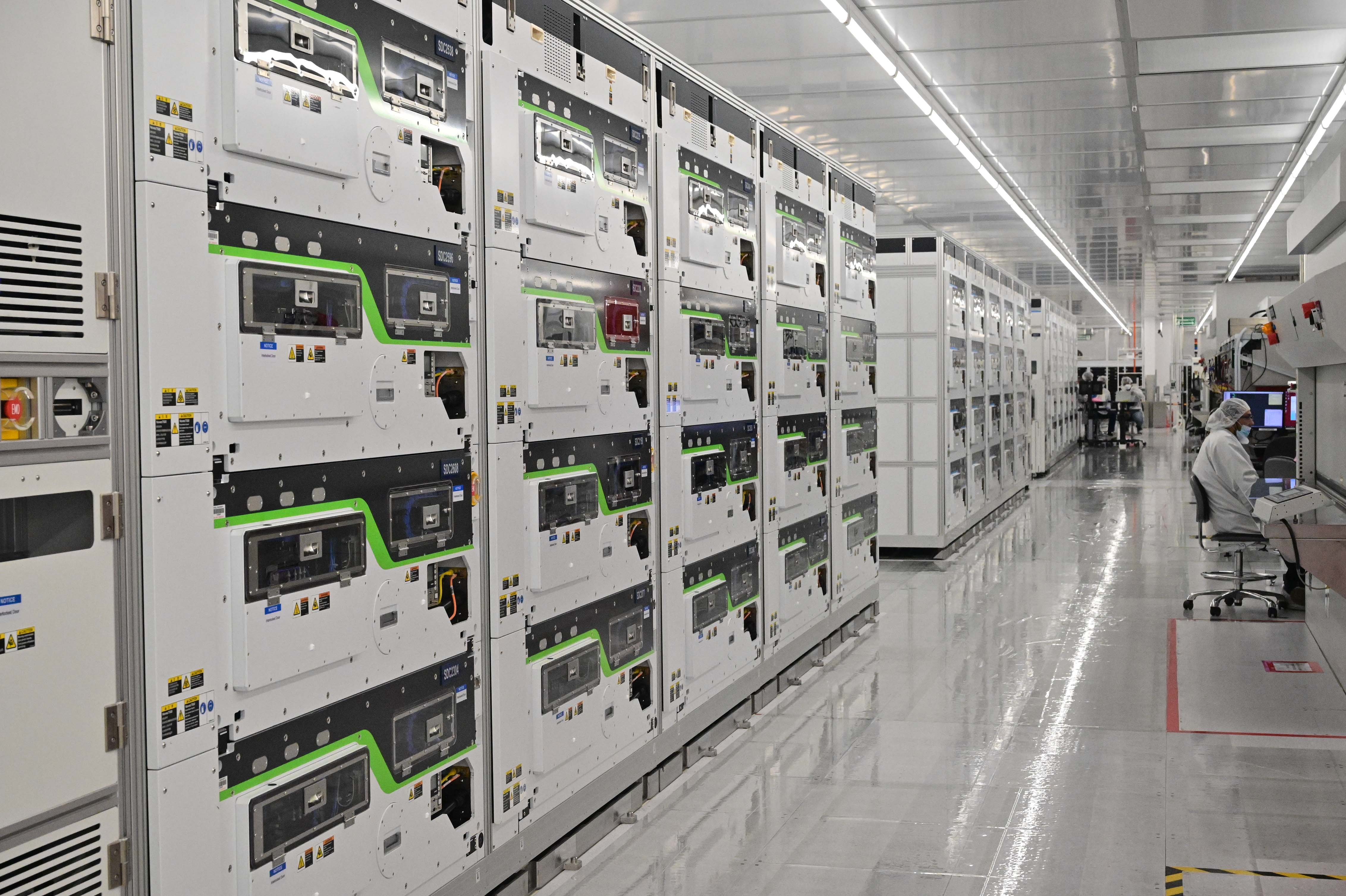
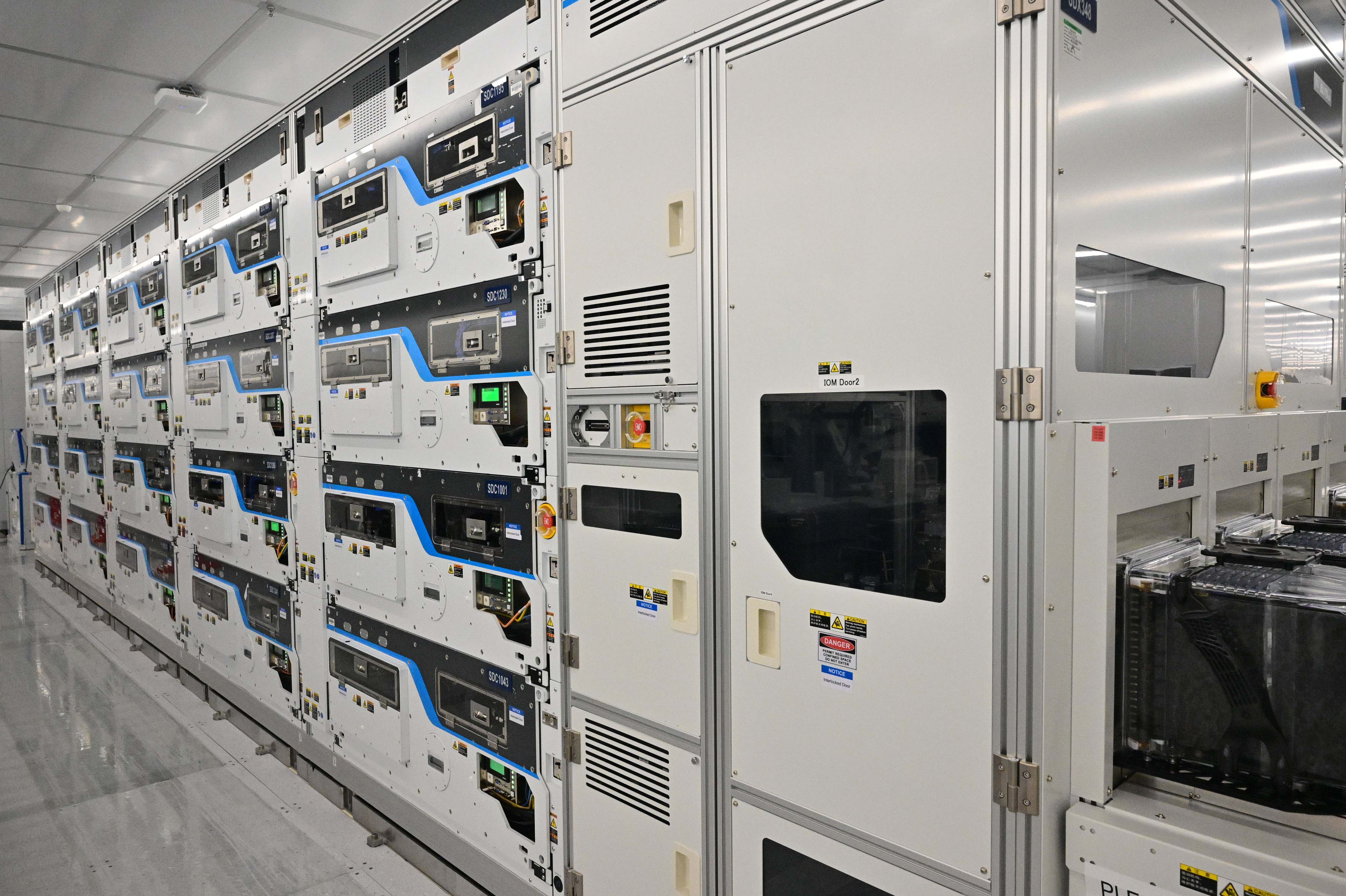
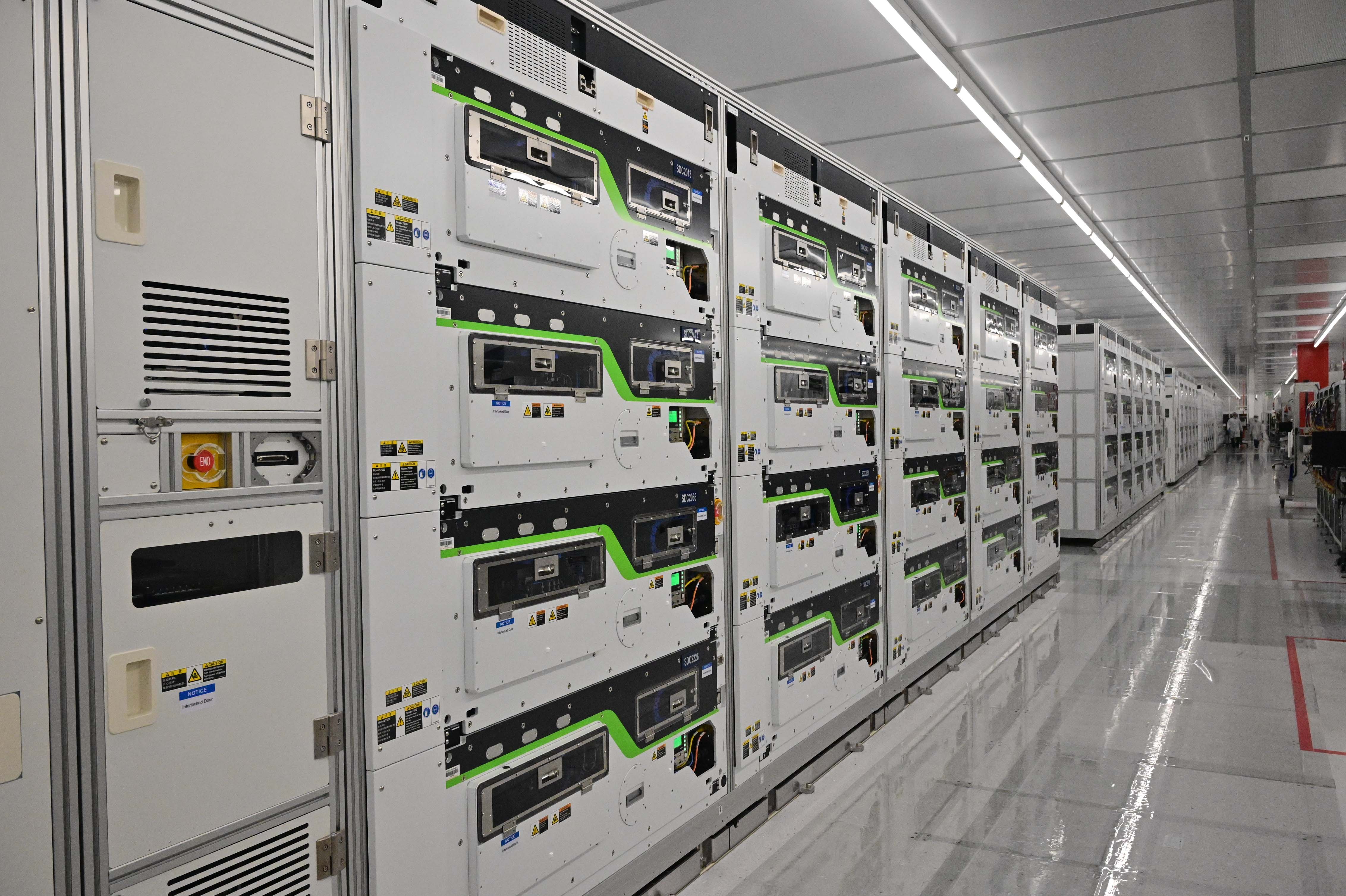
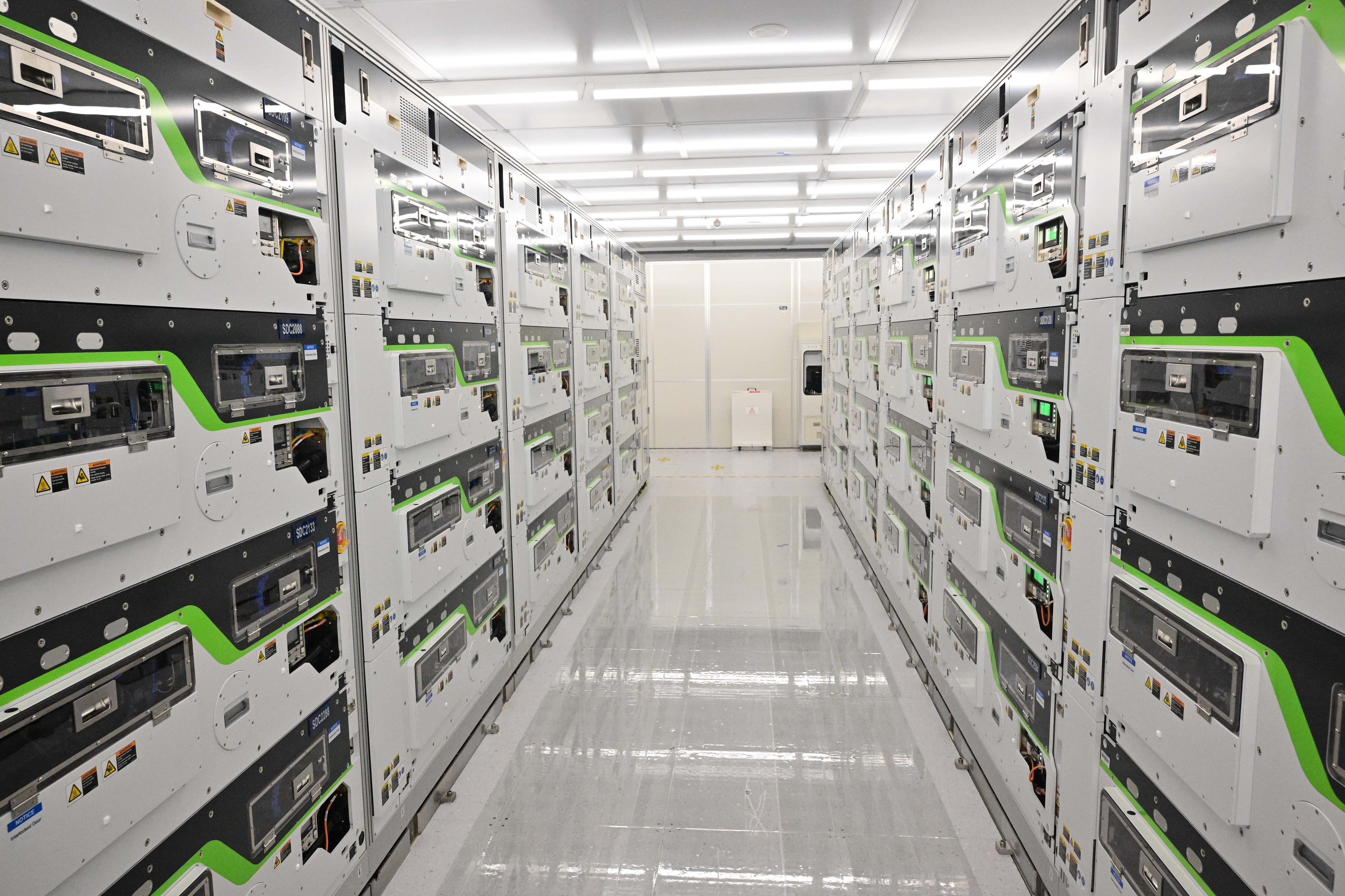
The die carriers are then moved by an automated guided vehicle (AGV - more below) to the sorting/test machines. These machines test the electrical characteristics of the chip circuits for reliability and defect analysis.
Each row of machines has 20 individual test cells, identifiable as distinct units in the first image in the album below, that weigh over 1,000 pounds and appear to be roughly three feet tall and six feet long. These test cells are arranged into five columns per machine, each with four stacked test cells, thus allowing 20 dies to be tested simultaneously in each group.
Each unit is assigned one die carrier's worth of dies to test, which occurs serially, and the number of dies per carrier varies based on type and size. The die carriers are slotted into one end of the machine and automatically moved internally to one of the test cells. Naturally, the production rate of these machines is a closely guarded secret.
There is a seemingly unending number of these large 20-unit machines in the facility, with rows upon rows working diligently in a massive floorspace, but we certainly weren't allowed to count the number of machines.
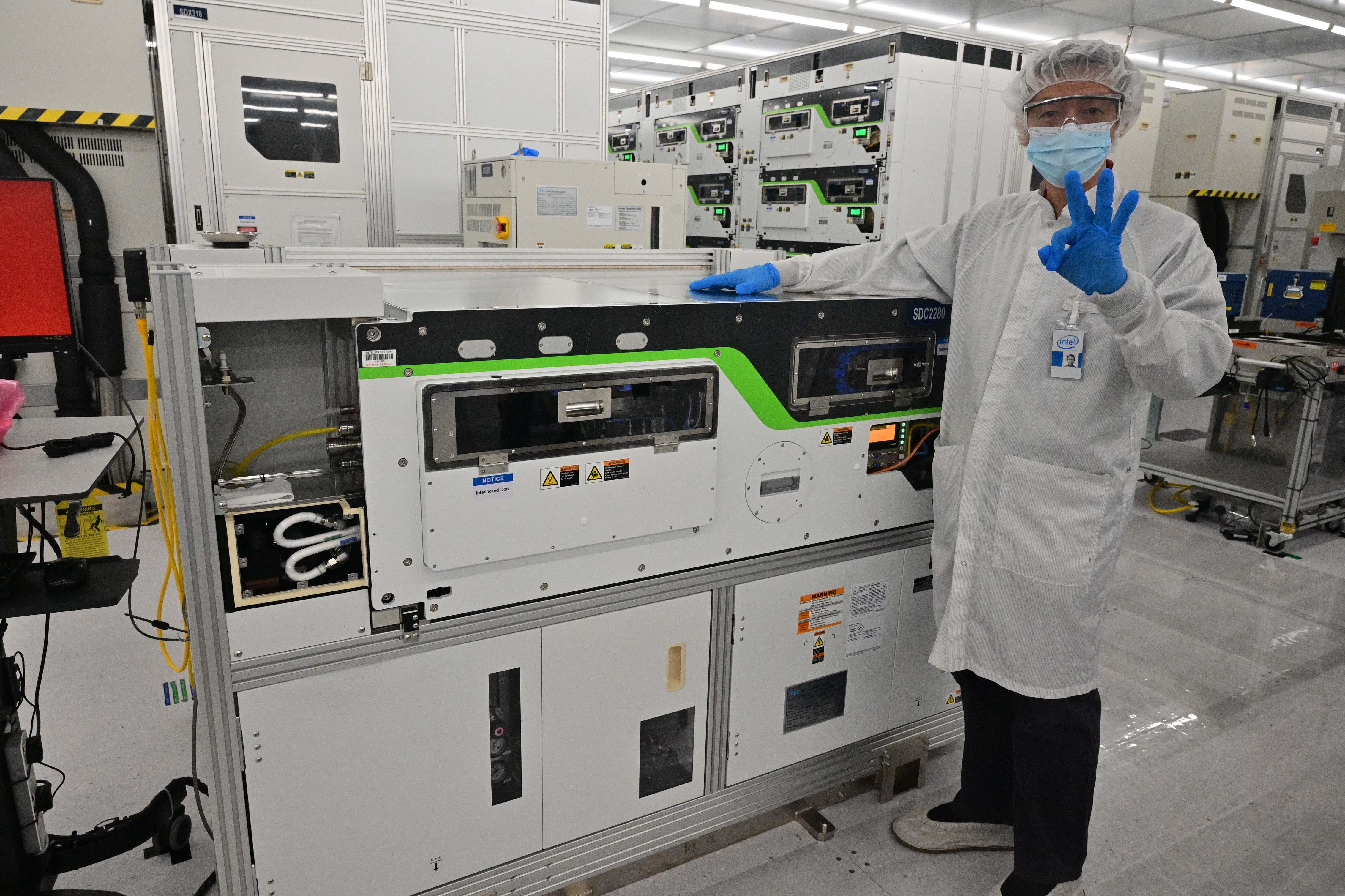
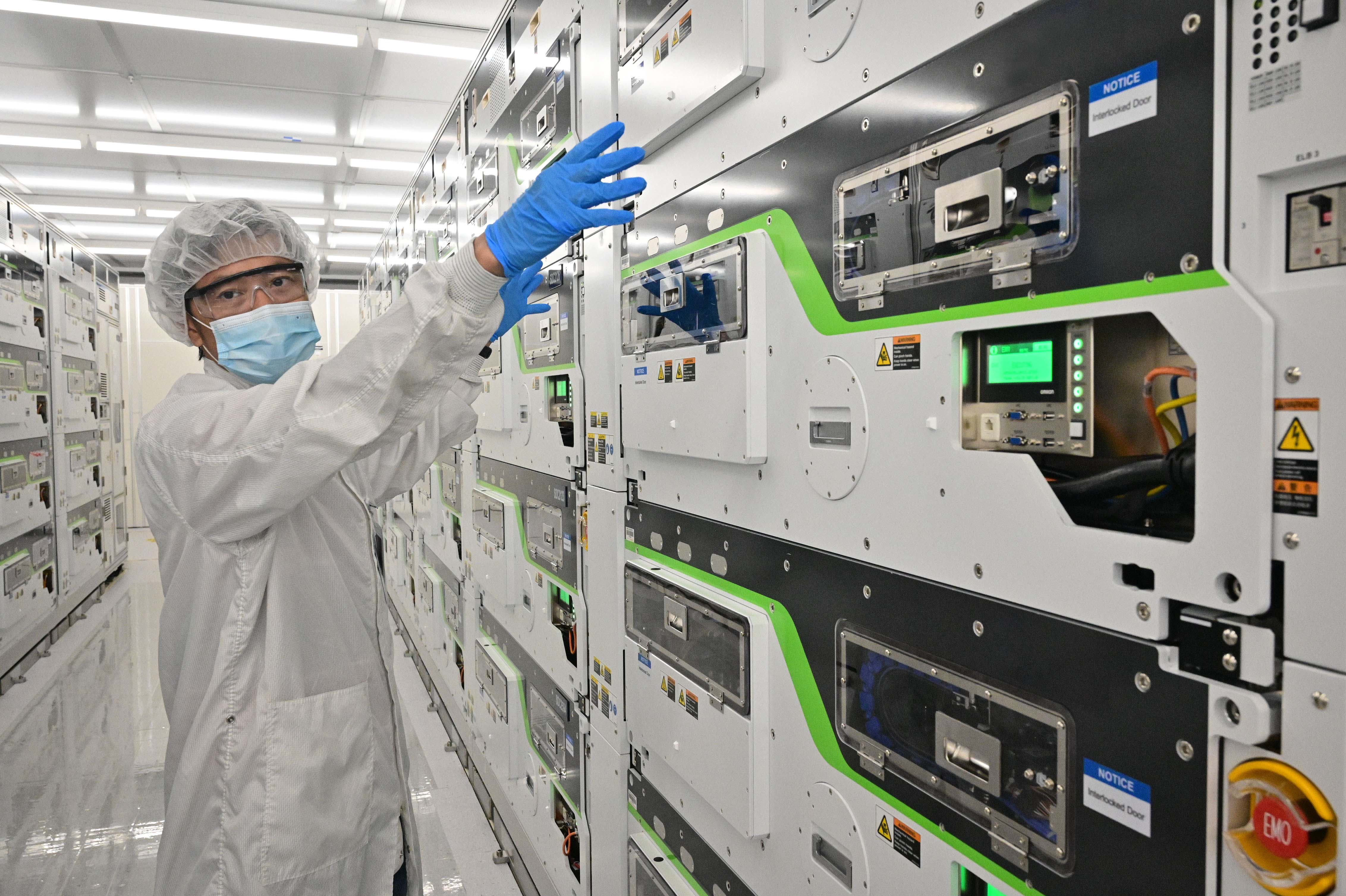
Here we can see an individual test cell outside of its larger housing. These hot-swappable units can be removed with a special lift to be repaired or inspected without interrupting the other 19 units in the group. The 1000-pound weight of each machine would be above the weight limit of the floor if Intel used traditional wheeled lifts, so these lifts float on a cushion of air, just like a hovercraft, to distribute the weight evenly across the floor. These transport machines can be pushed and maneuvered quite easily by a single person.
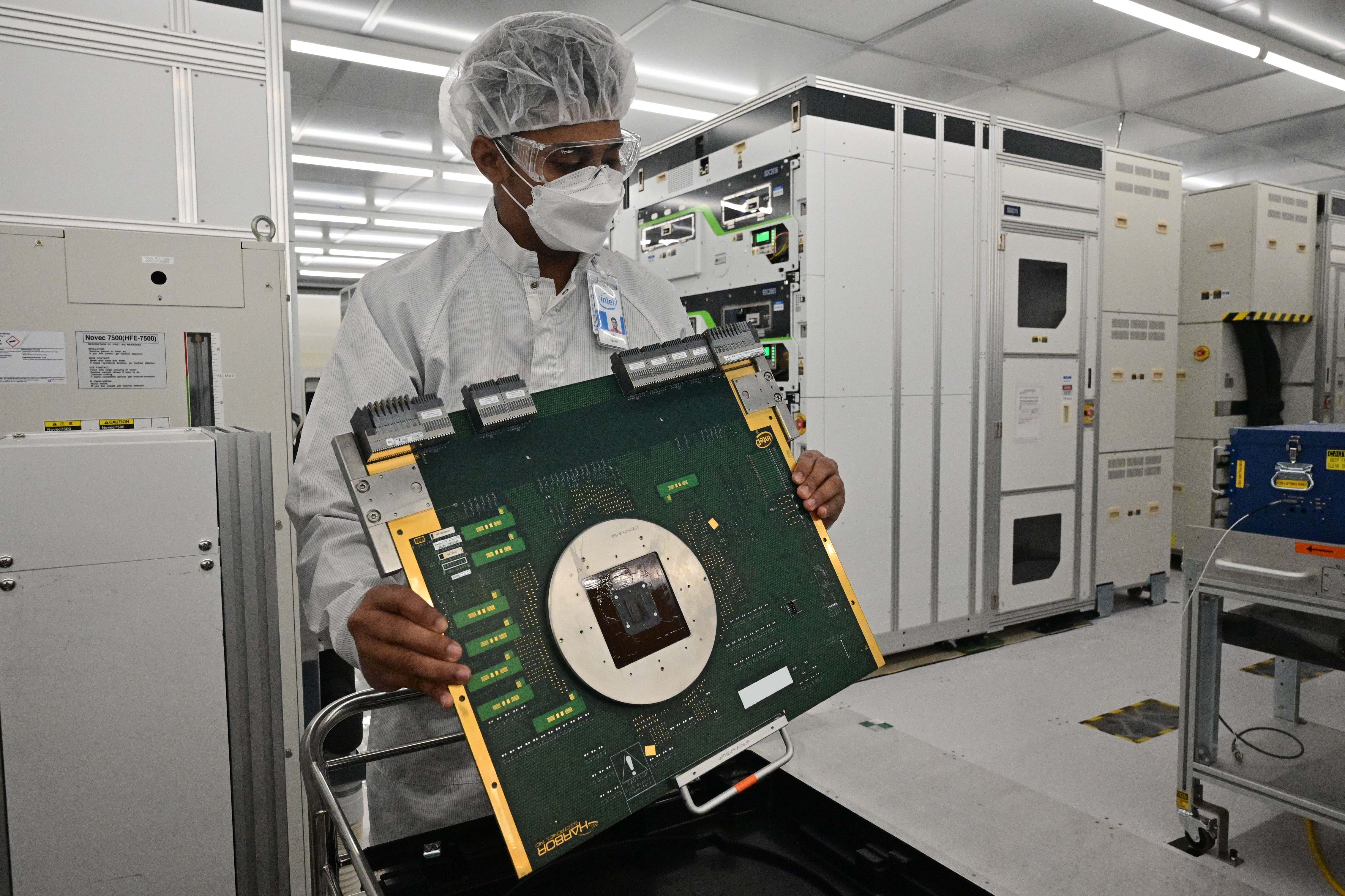
The third image shows a test board that resides inside each test cell. Each of these boards has a 'socket' with ~2,000 hair-like pins that mate with the die to put it through a battery of tests. Intel produces these custom test boards and machines at its System Integration and Manufacturing Services (SIMS) facility, which we'll cover below. These boards can test multiple types of dies without swapping the internal test board.
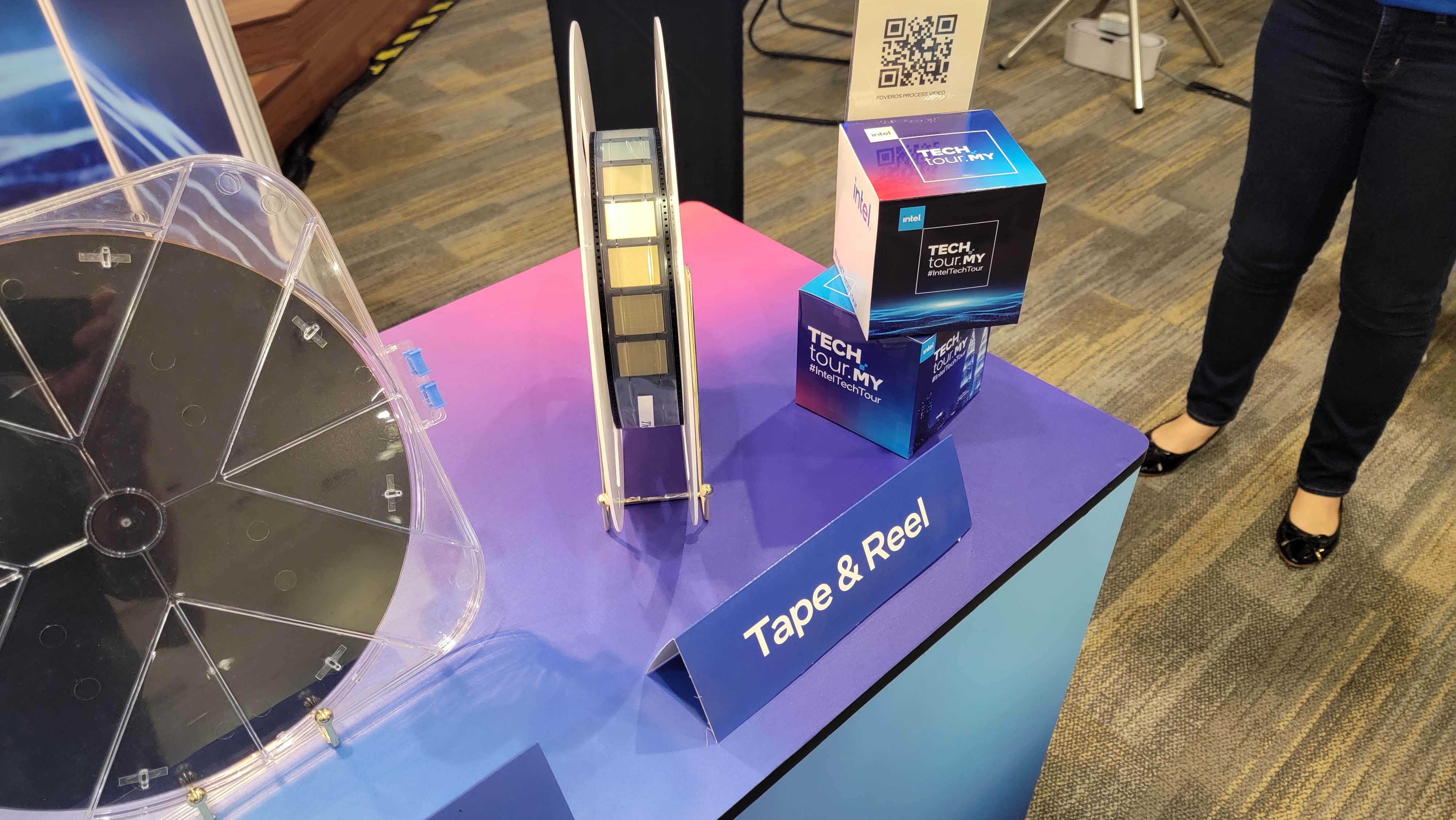
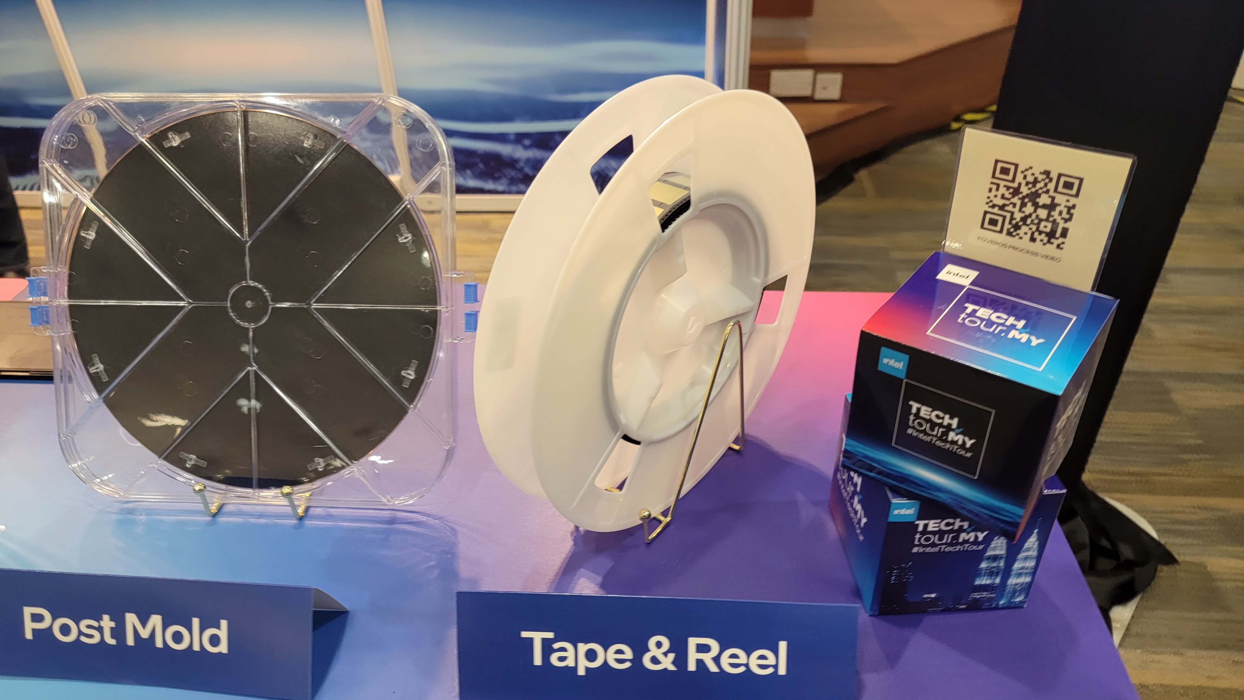
After testing, functional dies are sent to be placed onto reels for transport to the next production facility. These reels are much like a cassette tape, with dies attached at set intervals to the ribbon wound around the spindle.
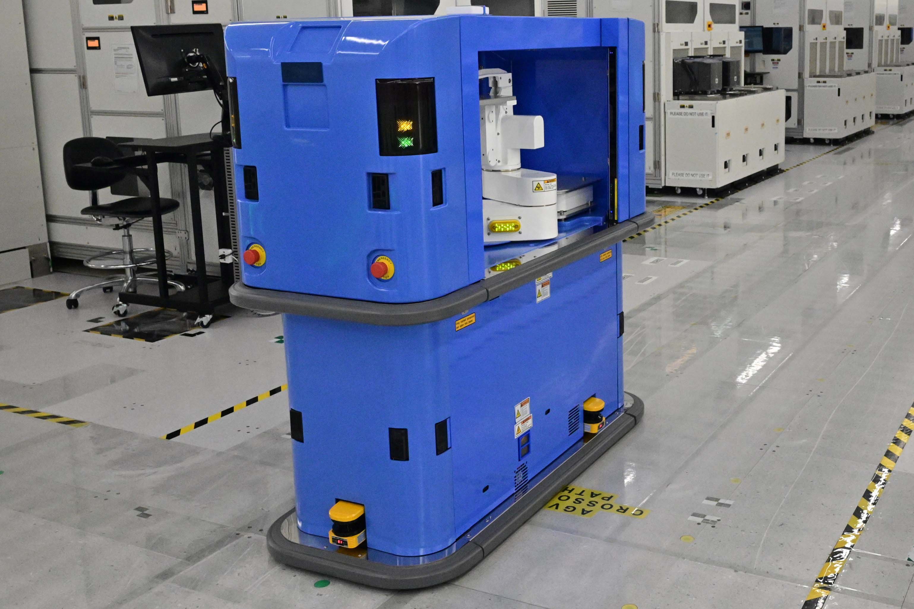
They weren't shown much in the images above, but an army of these automated guided vehicles (AGV) travels through the aisles continuously, shuffling FOUPS of wafers/dies between the machines as they travel on a cushion of air, just like the test unit lifter.
The AGVs have a robot arm in the middle of the unit, which is used to retrieve the FOUPS from mechanized storage units on the walls lining the production floor. The AGV then transports the FOUP to its destination and loads it into the test machines. As you can see in this video, Intel uses automated track-guided ceiling transport for FOUPS at some of its facilities, while AGVs are used at other facilities based on cost and cycle time requirements.
The AGVs have an assortment of sensors on each corner to prevent collisions with other AGVs or humans, but it appears the finer details of the sensors have been edited out of the image. Each electrical AGV can run for approximately an hour before it has to return to a charging station, perhaps partially explaining the sheer number of units on the production floor.
Instead of a pulsating beeping like you would hear from a school bus, these machines play a musical series of beeps as they coast around the floor to warn humans of their presence. The fleet of AGVs is controlled via automated software that routes the machines under the careful eye of a central human controller. All FOUPs have RFID tags to make sure they're carefully tracked during their travels.
Get Tom's Hardware's best news and in-depth reviews, straight to your inbox.
Current page: Kulim Die Sort and Die Preparation (KMDSDP)
Prev Page The Big Picture Next Page Penang Assembly and Test (PGAT)
Paul Alcorn is the Editor-in-Chief for Tom's Hardware US. He also writes news and reviews on CPUs, storage, and enterprise hardware.
-
Roland Of Gilead "If successful, those advanced nodes will grant Intel the lead over TSMC for the first time in years, " - so, the reasoning being here, that TSMC will be standing by scratching their arses during this same period. And thus Intel will overtake them!? Okay.Reply -
Paul Alcorn https://fuse.wikichip.org/news/7375/tsmc-n3-and-challenges-ahead/Reply
Intel will match TSMCs std cell density with the Intel 4 process by the end of this year. After that, roadmap projections indicate Intel will pull ahead. -
jkflipflop98 ReplyRoland Of Gilead said:"If successful, those advanced nodes will grant Intel the lead over TSMC for the first time in years, " - so, the reasoning being here, that TSMC will be standing by scratching their arses during this same period. And thus Intel will overtake them!? Okay.
No, you just inserted your own thoughts. No one is saying TSMC is going to stand still. We're saying they aren't going to be able to keep up. -
vertuallinsanity Intel utilized TMSC as a stand-in *partner* during a period of machinery teething issues.Reply
The intention of that partnership, for certain products, was always temporary in nature or Intel would have gone fab-less similar to AMD. Intel utilized TSMC to prevent bring-to-market delay while simultaneously reworking their fab processes and equipment to a viable state.
The article seems to imply TSMC makes their own processors or gpus and they're in direct competiton with Intel. They don't and they arent.
TSMC and/or Intel may trade process enhancement "blows" but Intel makes Intel CPUs for Intel and TSMC makes 'em for "anybody".
The article implication could apply to Apple, NVidia, AMD or others competing with Intel on similar node products.
Intel will continue to work with TSMC on GPUs and other product lines deemed fiscally feasible. Intel and TSMC are still partners.
There is no way anyone from Tom's hardware was allowed a tour of Intel's new ish.
Fact.. -
Roland Of Gilead Reply
No, you just inserted your own thoughts, in relation to my post!jkflipflop98 said:No, you just inserted your own thoughts. No one is saying TSMC is going to stand still. We're saying they aren't going to be able to keep up.
If you didn't notice, this article is one sided! I did certainly enjoy the tour and article in relation to Intel's tech, but there is zero context as to why TSMC 'might' fall behind.
You are right, no one is saying TSMC is gonna fall behind, but without context how is a reader supposed to know that? By checking the forums posts for an addendum article that gives the reasons why TSMC might fall behind? A bit of balance to illustrate these comments would help. -
td47 It would be interesting to know how Intel prevents IP and manufacturing methods/secrets from being exfiltrated from the Chengdu facility in China - given that country's penchant f or stealing and copying the Western Tech to try to catch up!Reply