Intel Demonstrates STT-MRAM for L4 Cache
Intel is caching up
Get Tom's Hardware's best news and in-depth reviews, straight to your inbox.
You are now subscribed
Your newsletter sign-up was successful

Intel researchers have demonstrated 2MB magnetic random-access memory (MRAM) arrays that fulfill the requirements for application as an on-chip L4 cache, which include data retention, endurance and bit error rates. The work marks a step forward for the technology.
Spin-transfer torque magnetic random-access memory (STT-MRAM) is a non-volatile memory (it retains its memory state when power is turned off) that consists of one magnetic junction and one transistor. It is compatible with standard CMOS technology, and together with its other characteristics such as speed, endurance, and density, it has gained interest in the industry. Commercial feasibility to date has primarily been focused on MRAM as off-chip embedded non-volatile memory (eNVM).
Intel has now built and demonstrated 2MB arrays of STT-MRAM that are capable of meeting on-chip L4 cache specifications, Intel claimed. An L4 cache would have looser performance requirements, but higher capacity than lower level caches, which usually consist of six-transistor SRAM cells. Compared to eNVM, it imposes more stringent characteristics in terms of speed, density and endurance.
Article continues belowIntel reported a 20ns write time, 4ns read time, endurance of 10E12 cycles and memory retention of one second at 110 degrees Celsius for the MRAM chips. The bit error rates were reportedly also good enough so they could be handled with error-correcting code (ECC) techniques.

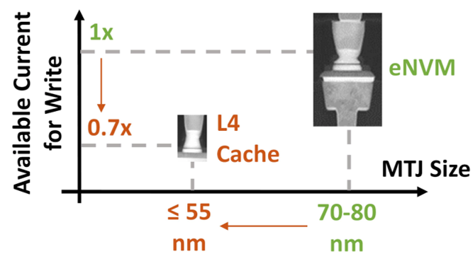
Some process optimizations were necessary to meet the requirements for an L4 cache. The MRAM bitcell had to be scaled down compared to the eNVM. The magnetic junction was scaled from 70-80nm to 55nm, although this came at the expense of a reduced maximum writing current. The researchers also optimized the material stack of the device.
It is likely the research was conducted on Intel’s 22FFL process (the same process as used for Foveros and Intel’s recent Horse Ridge quantum control chip), as the company announced earlier this year that both MRAM and RRAM (resistive RAM) were production-ready with a bit yield reportedly greater than 99.9%.

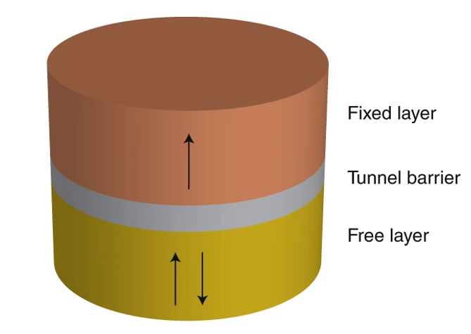
In general, STT-MRAM stores bits through the variable resistance state of the cell. This is accomplished by its magnetic tunnel junction (MTJ). An MTJ consists of magnetic fixed and free layers, separated by a tunnel barrier. The relative alignment of the fixed and free layer’s magnetic direction determines the MTJ’s resistance. For example, a parallel alignment of their magnets orientation would result in a low resistance state. The magnetization of the free layer can be changed through the spin-transfer torque effect by driving a current across the junction.
Get Tom's Hardware's best news and in-depth reviews, straight to your inbox.
The work was presented at the annual International Electronic Devices Meeting (IEDM) in San Francisco and described in Nature. Intel is not the only company working on STT-MRAM. The list includes Everspin, Samsung, TSMC, and GlobalFoundries.
-
Rdslw now lets talk numbers. 2MB does not seem impressive.Reply
BUT its just POC, if they can make it to 300MB+ (like epics L3) and as mentioned 20ns @ 2MB that scales same way as L3 does, now that would be something in my eyes.
its up to them now how generously L4 will be used, and how it affects real live performance. -
bit_user ReplyIntel reported a 20nm write time, 4ns read time, endurance of 1012 cycle
As noted above, the units on the first metric should certainly be ns. However, I'm more puzzled & troubled by the endurance figure... -
bit_user Reply
It seems to me that the main advantages of MRAM are its size and power. Here, being a semi-passive technology could be a huge win for energy efficiency. Both serve as constraints on scaling cache sizes, using current technology.Rdslw said:now lets talk numbers. 2MB does not seem impressive.
BUT its just POC, if they can make it to 300MB+ (like epics L3) and as mentioned 20ns @ 2MB that scales same way as L3 does, now that would be something in my eyes.
its up to them now how generously L4 will be used, and how it affects real live performance. -
Rdslw Reply
thanks, I did not notice power is such an issue in this case, as its constantly refreshed. Then it becomes semi-constant (propably we could idle on half the current power or even lower?). Even more reasons to wait to see real results.bit_user said:It seems to me that the main advantages of MRAM are its size and power. Here, being a semi-passive technology could be a huge win for energy efficiency. Both serve as constraints on scaling cache sizes, using current technology.
so AMD is becoming king of killing "heavy LOAD"
while INTEL is trying to be good at IDLE.
interesting times indeed.