Nvidia Unveils Its Next-Generation 7nm Ampere A100 GPU for Data Centers, and It's Absolutely Massive
7nm and 54 billion transistors
Get Tom's Hardware's best news and in-depth reviews, straight to your inbox.
You are now subscribed
Your newsletter sign-up was successful
The day has finally arrived for Nvidia to take the wraps off of its Ampere architecture. Sort of. While Ampere will inevitably make its way into some of the best graphics cards and find a place on our GPU hierarchy, today's digital GTC announcement is only about the Nvidia A100, a GPU designed primarily for the upcoming wave of exascale supercomputers and AI research. It's the descendant of Nvidia's existing line of Tesla V100 GPUs, and like Volta V100 we don't expect to see A100 silicon in any consumer GPUs. Well, maybe a Titan card—Titan A100?—but I don't even want to think about what such a card would cost, because the A100 is a behemoth of a chip.
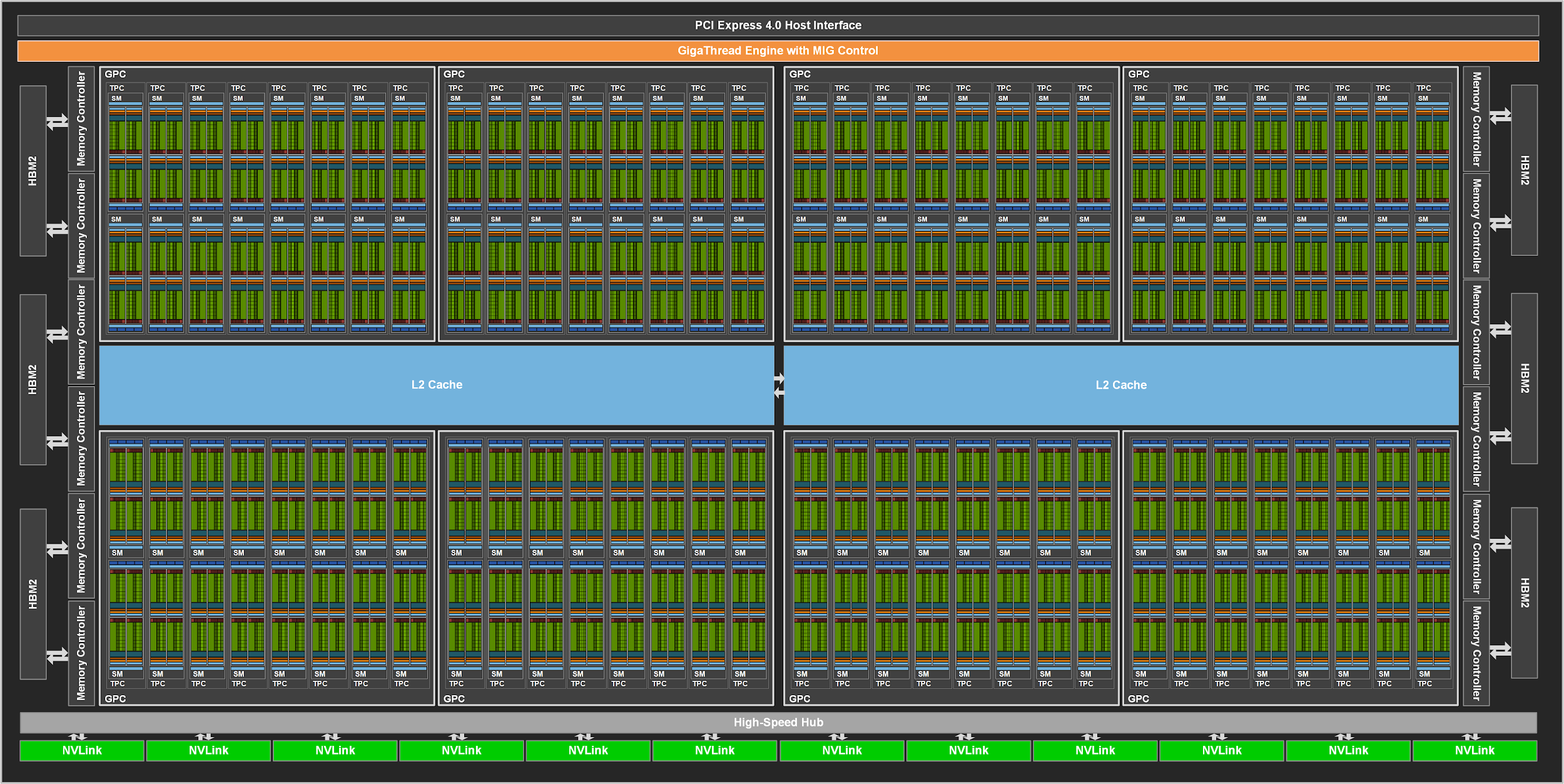
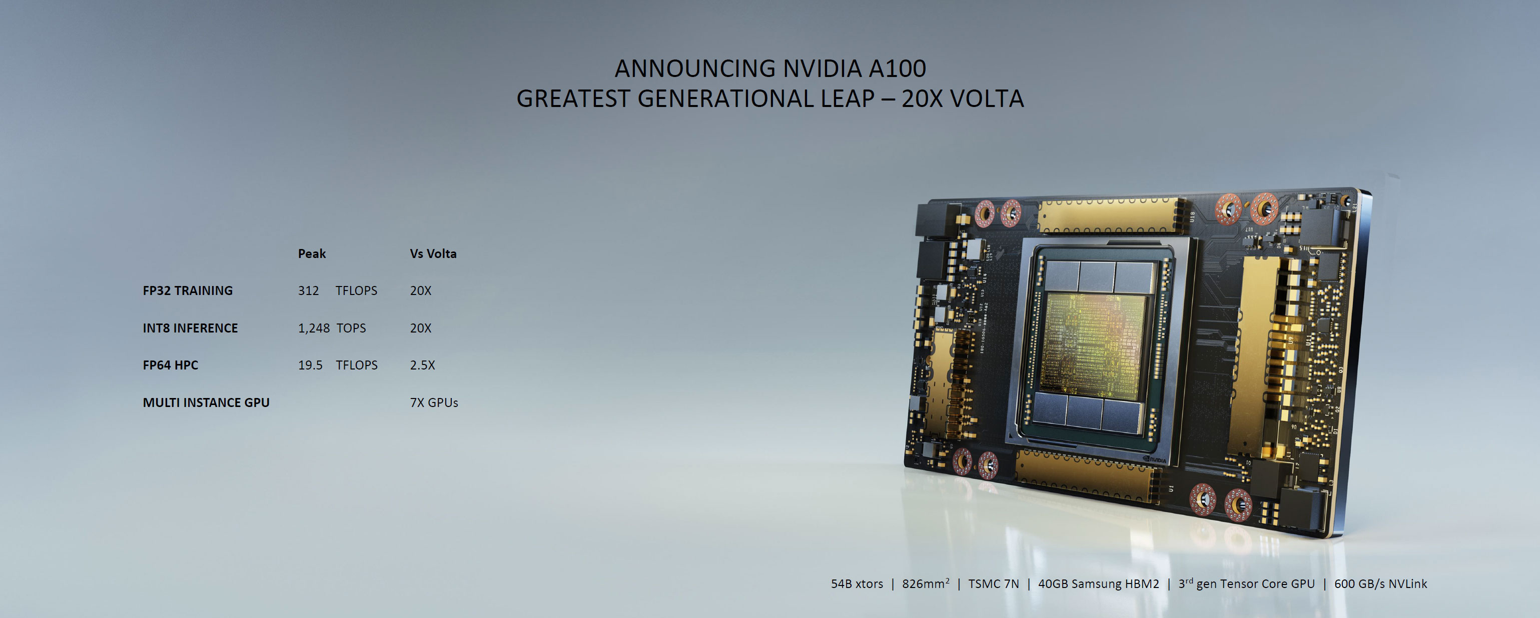
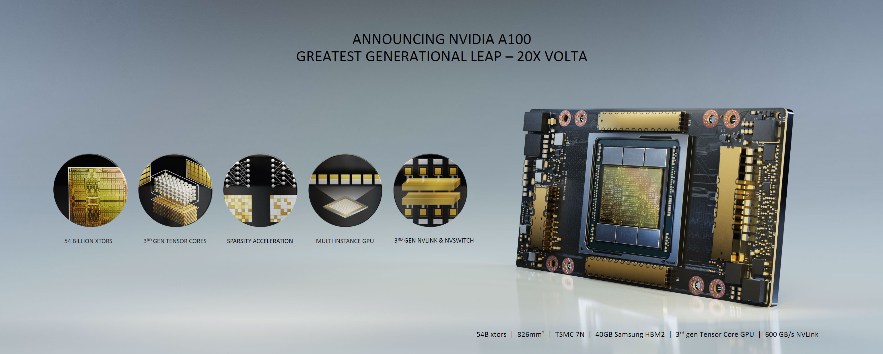
Let's start with what we know at a high level. First, the Nvidia A100 will pack a whopping 54 billion transistors, with a die size of 826mm square. GV100 for reference had 21.1 billion transistors in an 815mm square package, so the A100 is over 2.5 times as many transistors, while only being 1.3% larger. Nvidia basically couldn't make a larger GPU, as the maximum reticle size for current lithography is around 850mm square. The increase in transistor count comes courtesy of TSMC's 7nm FinFET process, which AMD, Apple, and others have been using for a while now. It's a welcome and necessary upgrade to the aging 12nm process behind Volta.
Along with the monster GPU itself are six stacks of HBM2 memory, which Nvidia says provide 40GB of total memory capacity. Since HBM2 stacks come in power of two size increments (i.e., 8GB per stack), we can only assume one of the stacks is for either redundancy of some form and/or future products. We specifically asked and got a vague answer saying, "We're only shipping products with five HBM2 stacks right now." Whether the sixth stack simple doesn't exist on current actual A100 boards, or is a dummy spacer, or is simply disabled ... Nvidia wouldn't say. But at some point, Nvidia plans to have A100 solutions that do support six HBM2 stacks and probably with more SMs enabled (more on that below).
Article continues belowFor HPC (high performance computing) nodes in a super computer, Nvidia also upgraded the NVLink to 600GB/s for each GPU, and NVSwitch provides full speed connections to any other node in a server. 8-way Nvidia A100 systems already exist and have been shipped to customers including the Department of Energy. These use six NVSwitch controllers with an aggregate 4.8 TBps of bandwidth.
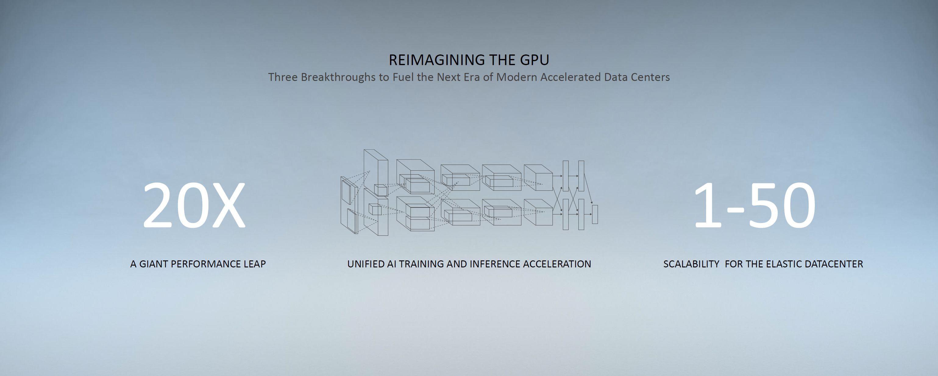
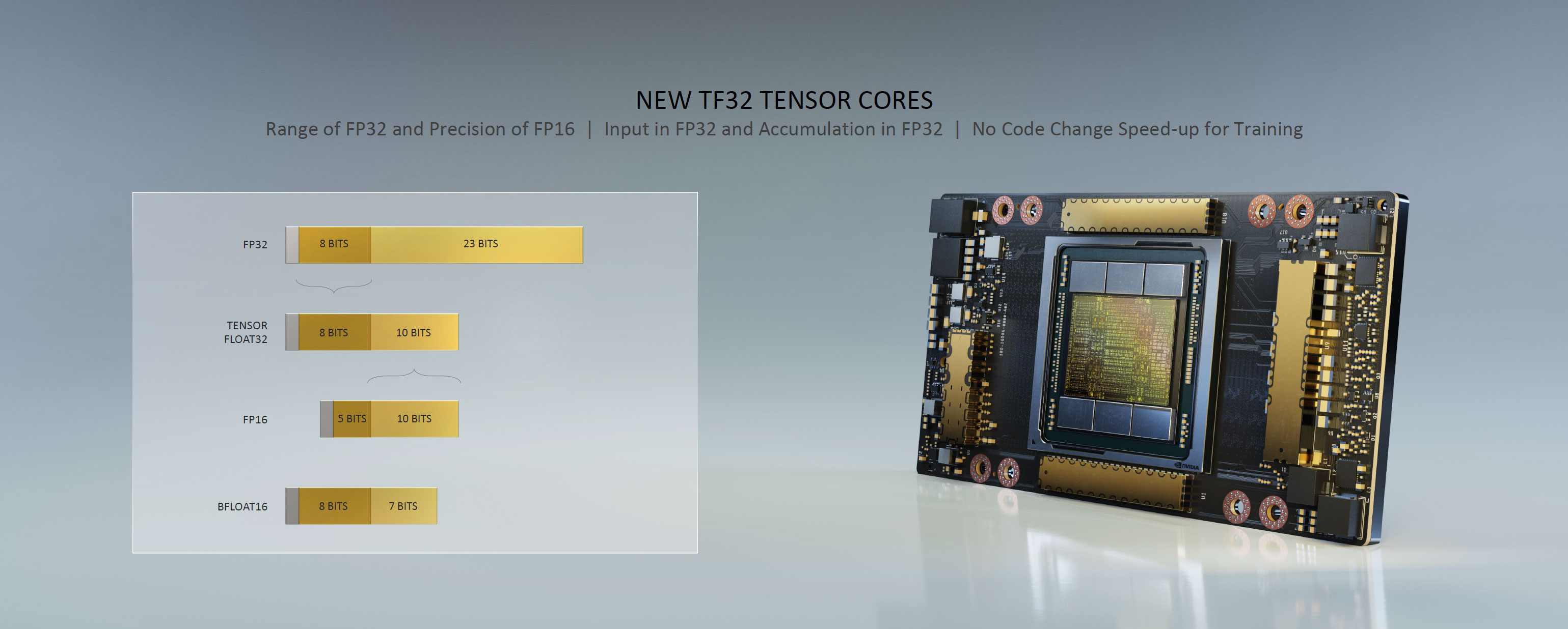
The Nvidia A100 isn't just a huge GPU, it's the fastest GPU Nvidia has ever created, and then some. The third generation Tensor cores in A100 provide a new hybrid FP32 format called TF32 (Tensor Float 32, which is basically like Google's bfloat16 format, with three extra bits of significant digits) that aims to provide a balanced option with the precision of FP16 and exponent sizes of FP32. For workloads that use TF32, the A100 can provide 312 TFLOPS of compute power in a single chip. That's up to 20X faster than the V100's 15.7 TFLOPS of FP32 performance, but that's not an entirely fair comparison since TF32 isn't quite the same as FP32.
Elsewhere, the A100 delivers peak FP64 performance of 19.5 TFLOPS. That's more FP64 performance than the V100's FP32, and about 2.5 times the FP64 performance. However, Nvidia says that the third generation Tensor cores support FP64, which is where the 2.5X increase in performance comes from. The Tensor cores aren't be the same instruction set as FP64 CUDA cores, so if you're looking for CUDA FP64 performance it's 'only' 9.7 TFLOPS.
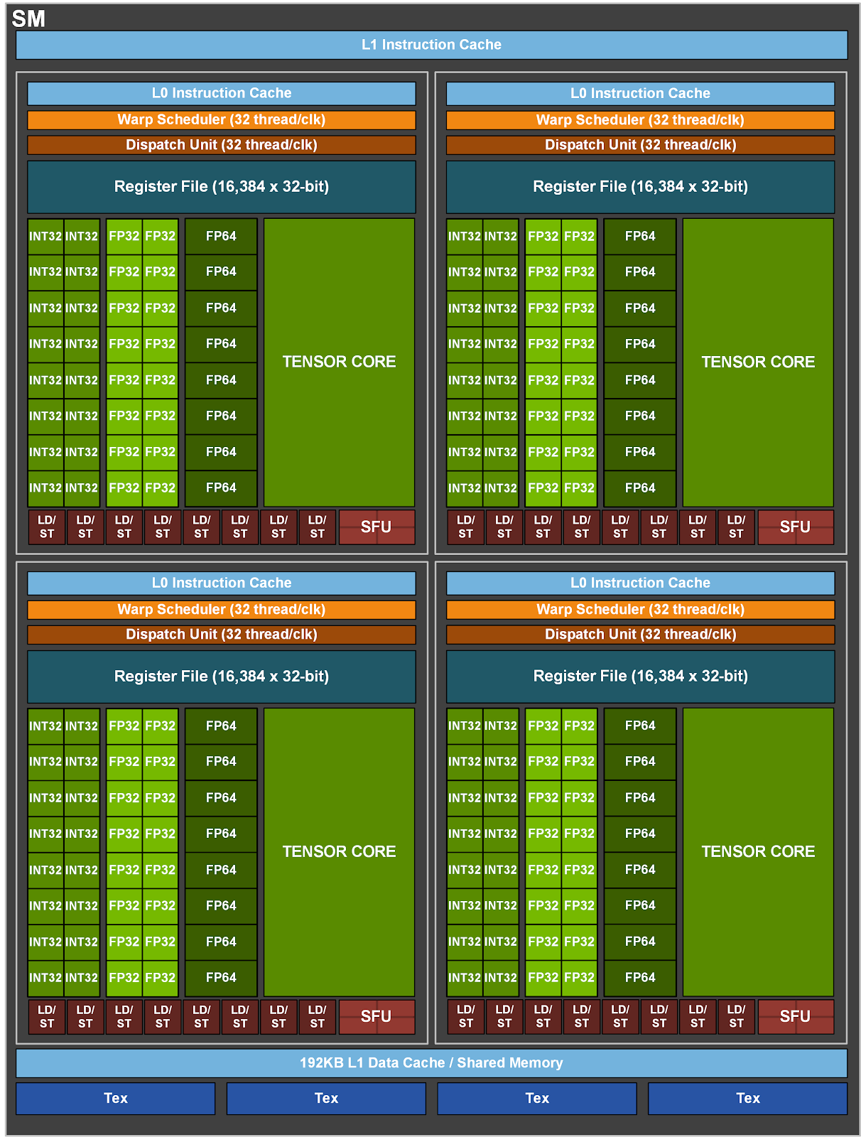
Nvidia has now posted the specs of the A100 chip, and the details are ... surprising. First, the new Tensor cores are a significant change from the previous generation. There are only four Tensor cores per SM (compared to 8 on Volta and Turing), but those four cores deliver twice the performance of the previous generation's eight cores. The image on Nvidia's site showing the new SM is called "New GA100 SM with Uber Tensor Core.png" which pretty much says it all.
Get Tom's Hardware's best news and in-depth reviews, straight to your inbox.
Something else to note: The full A100 chip has up to 128 SMs and 8192 FP32 CUDA cores, but only 108 SMs are enabled in the initial version. That says a lot about yields on such a massive chip, as well as TSMC's N7P node. Nvidia is probably saving up 'good' die for future products, but the initial A100 will only have about 85% of the SMs enabled (compared to 95% of SMs being enabled on the V100). There must be a massive amount of redundancy built into the critical paths to allow such a chip to exist and function at all.
One interesting tidbit that never came up in the announcement: ray tracing. The Volta V100 also skipped ray tracing, partly because it came before Turing but also because it was focused on delivering compute above all else. Given the above block diagrams, it appears the A100 follows a similar path and leaves RT cores for other Ampere GPUs. It's yet another clear indication that A100 isn't for consumers and probably won't even go into a Titan card. Or maybe we'll get a Titan A100 for entry-level compute and deep learning or whatever.
Looking at the details of the SM, we get a similar design to Volta V100: 64 FP32 cores and 64 INT32 cores, with the four large Tensor clusters. With 54 SMs enabled, the A100 has a total of 6912 FP32 CUDA cores, and the same for INT32, with half as many (3456) FP64 cores. But as noted above, the Tensor cores can also do FP64 calculations, yielding the same 19.5 TFLOPS of compute for both FP64 and FP32. Interesting to note is that FP16 performance is up to 78 TFLOPS, but BF16 is half that.
Here's the full specs table:
| Data Center GPU | NVIDIA Tesla P100 | NVIDIA Tesla V100 | NVIDIA A100 |
| GPU Codename | GP100 | GV100 | GA100 |
| GPU Architecture | NVIDIA Pascal | NVIDIA Volta | NVIDIA Ampere |
| GPU Board Form Factor | SXM | SXM2 | SXM4 |
| SMs | 56 | 80 | 108 |
| TPCs | 28 | 40 | 54 |
| FP32 Cores / SM | 64 | 64 | 64 |
| FP32 Cores / GPU | 3584 | 5120 | 6912 |
| FP64 Cores / SM | 32 | 32 | 32 |
| FP64 Cores / GPU | 1792 | 2560 | 3456 |
| INT32 Cores / SM | NA | 64 | 64 |
| INT32 Cores / GPU | NA | 5120 | 6912 |
| Tensor Cores / SM | NA | 8 | 4 |
| Tensor Cores / GPU | NA | 640 | 432 |
| GPU Boost Clock | 1480 MHz | 1530 MHz | 1410 MHz |
| Peak FP16 Tensor TFLOPS with FP16 Accumulate | NA | 125 | 312/624 |
| Peak FP16 Tensor TFLOPS with FP32 Accumulate | NA | 125 | 312/624 |
| Peak BF16 Tensor TFLOPS with FP32 Accumulate | NA | NA | 312/624 |
| Peak TF32 Tensor TFLOPS | NA | NA | 156/312 |
| Peak FP64 Tensor TFLOPS | NA | NA | 19.5 |
| Peak INT8 Tensor TOPS | NA | NA | 624/1248 |
| Peak INT4 Tensor TOPS | NA | NA | 1248/2496 |
| Peak FP16 TFLOPS | 21.2 | 31.4 | 78 |
| Peak BF16 TFLOPS | NA | NA | 39 |
| Peak FP32 TFLOPS | 10.6 | 15.7 | 19.5 |
| Peak FP64 TFLOPS | 5.3 | 7.8 | 9.7 |
| Peak INT32 TOPS | NA | 15.7 | 19.5 |
| Texture Units | 224 | 320 | 432 |
| Memory Interface | 4096-bit HBM2 | 4096-bit HBM2 | 5120-bit HBM2 |
| Memory Size | 16 GB | 32 GB / 16 GB | 40 GB |
| Memory Data Rate | 703 MHz DDR | 877.5 MHz DDR | 1215 MHz DDR |
| Memory Bandwidth | 720 GB/sec | 900 GB/sec | 1.6 TB/sec |
| L2 Cache Size | 4096 KB | 6144 KB | 40960 KB |
| Shared Memory Size / SM | 64 KB | Configurable up to 96 KB | Configurable up to 164 KB |
| Register File Size / SM | 256 KB | 256 KB | 256 KB |
| Register File Size / GPU | 14336 KB | 20480 KB | 27648 KB |
| TDP | 300 Watts | 300 Watts | 400 Watts |
| Transistors | 15.3 billion | 21.1 billion | 54.2 billion |
| GPU Die Size | 610 mm² | 815 mm² | 826 mm² |
| TSMC Manufacturing Process | 16 nm FinFET+ | 12 nm FFN | 7 nm N7 |
I've seen a few people prior to this announcement suggesting Nvidia will have Ampere GPUs running at upward of 2.0 GHz, maybe even as high as 2.5 GHz. Clearly, A100 isn't going that route, with a boost clock of 1410 MHz. All of the performance data discussed is also based on the boost clock, which the A100 may or may not maintain under heavy workloads. Nvidia tends to be conservative on its consumer boost clocks, but in the data center things aren't quite the same.
Power use for a single Nvidia A100 is 400W this round, 33% higher than the P100 and V100 iterations. The HBM2 memory is also clocked at 1215 MHz this round, which is a healthy 38% increase over the V100 and currently represents the fastest HBM2 implementation we've seen. As noted above, while the images show six HBM2 stacks, Nvidia's specs table says the HBM2 has a 5120-bit interface, which is five 1024-bit interfaces. Is an entire HBM2 stack disabled due to yields, or is it just a dummy chip for now? We suspect the former, but Nvidia did not confirm this, saying only that current products are shipping with five HBM2 stacks.
Let's reiterate that this GPU is not going into GeForce any time soon. Asked about the consumer line, Nvidia CEO Jensen Huang noted that Nvidia doesn't use HBM2 in consumer parts. We can safely assume there will be GDDR6-equipped Ampere GPUs at some point, but they won't be using the A100 silicon. Which, again, is fair enough. 826mm square and 40GB HBM2 with 1.6 TBps of bandwidth isn't something our consumer PCs really need right now, never mind the FP64 and TF32 clusters or the lack of RT cores.
[Obi-wan waves his hand: "These aren't the GPUs you're looking for."]
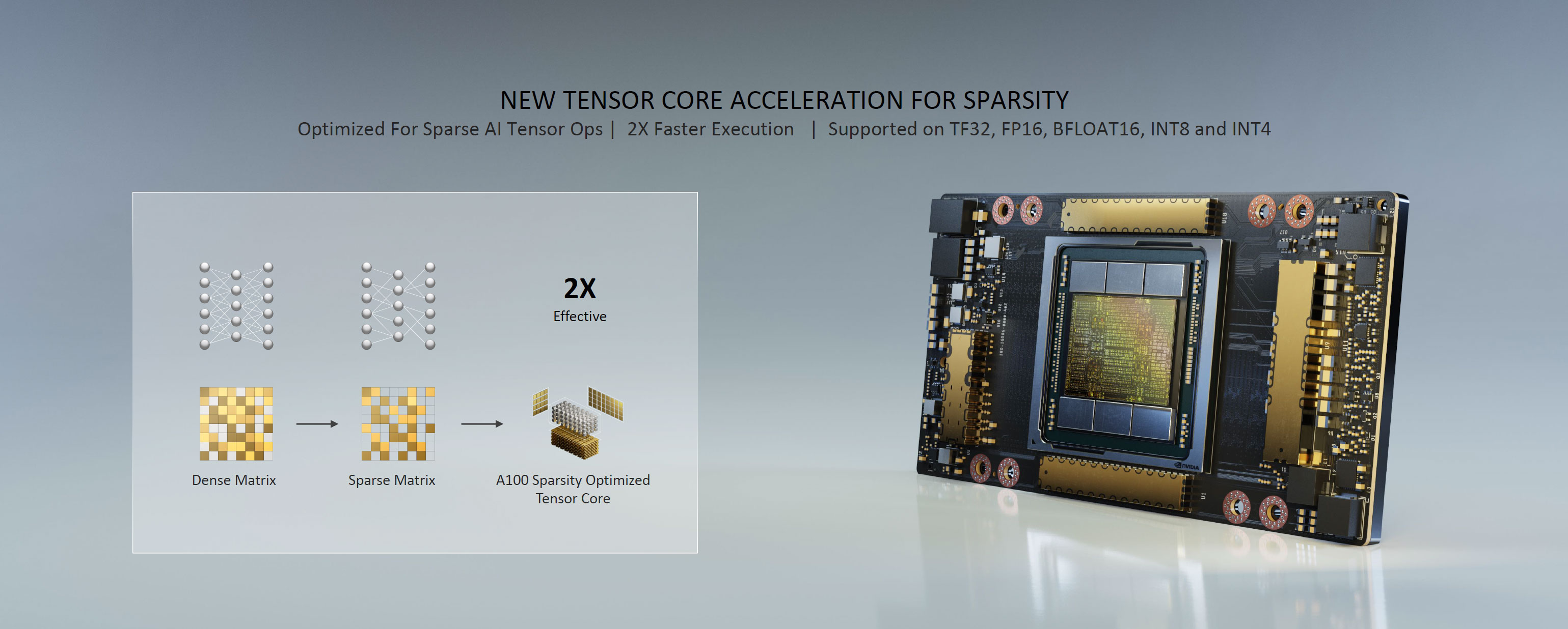
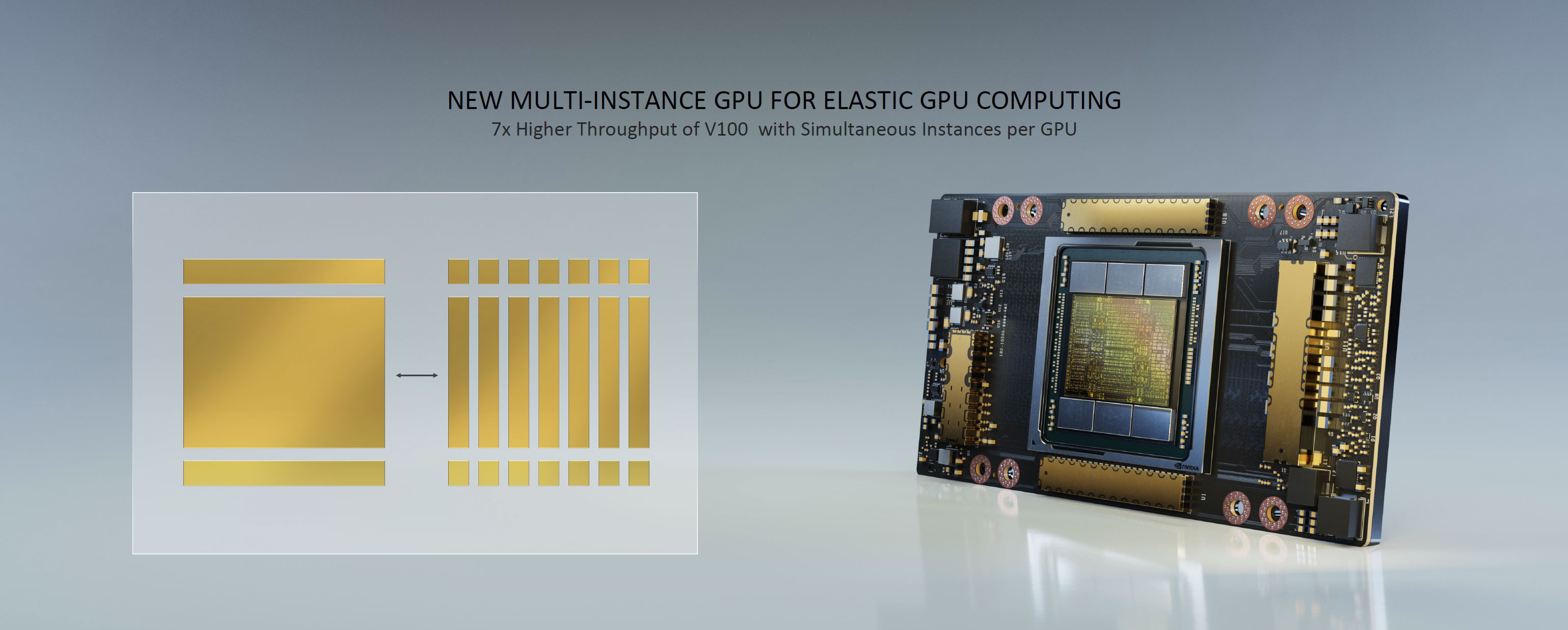
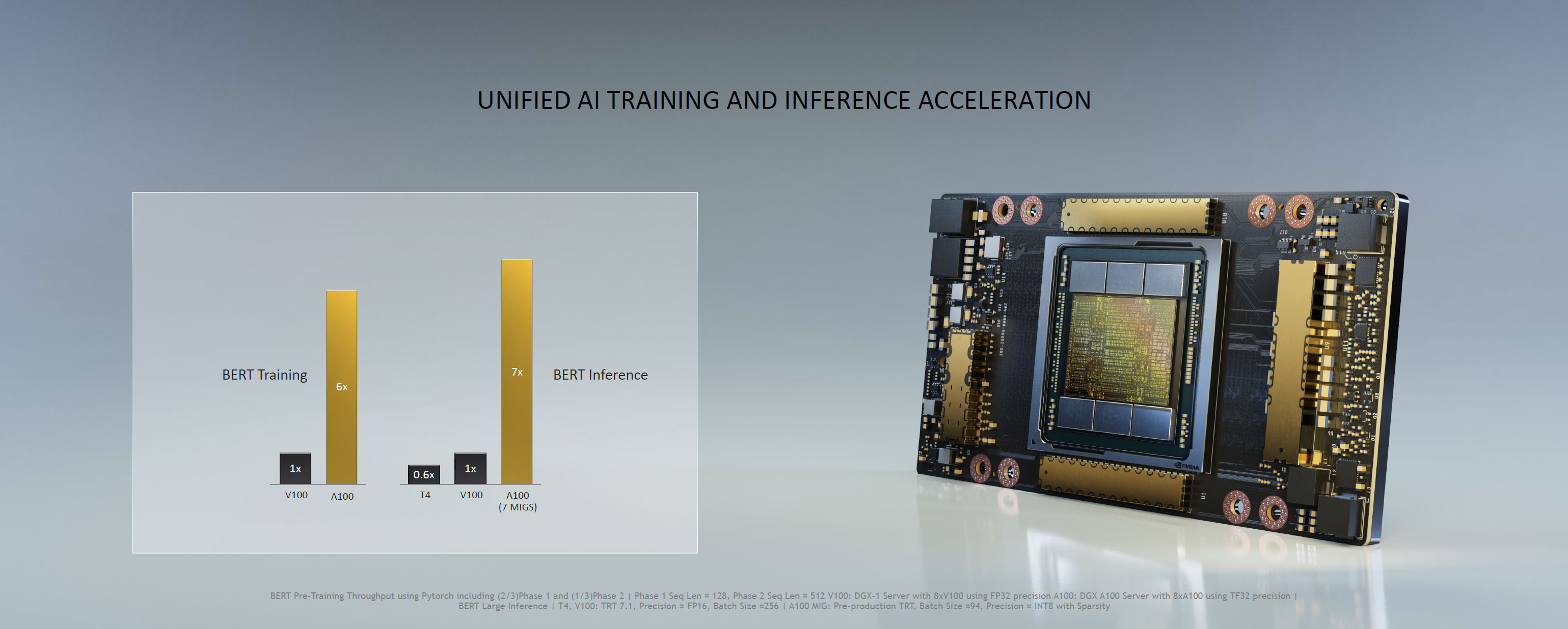
The Nvidia A100 should definitely deliver the goods for the target market, though. Along with other architectural enhancements including sparse matrix optimizations where it's (up to?) twice as fast as V100, the A100 has multi-GPU instancing that allows it to be partitioned into seven separate instances. For scale-out applications, then, a single A100 can have 7X the instancing performance of a V100 GPU.
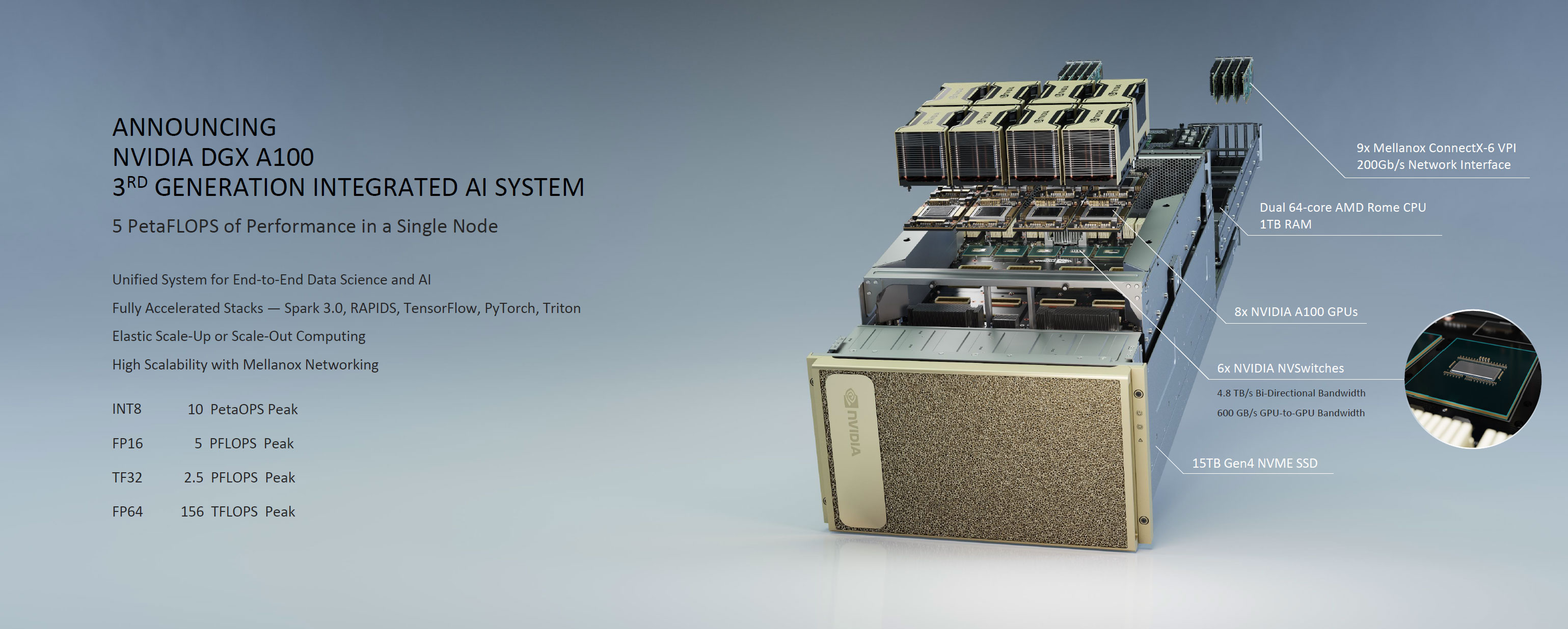
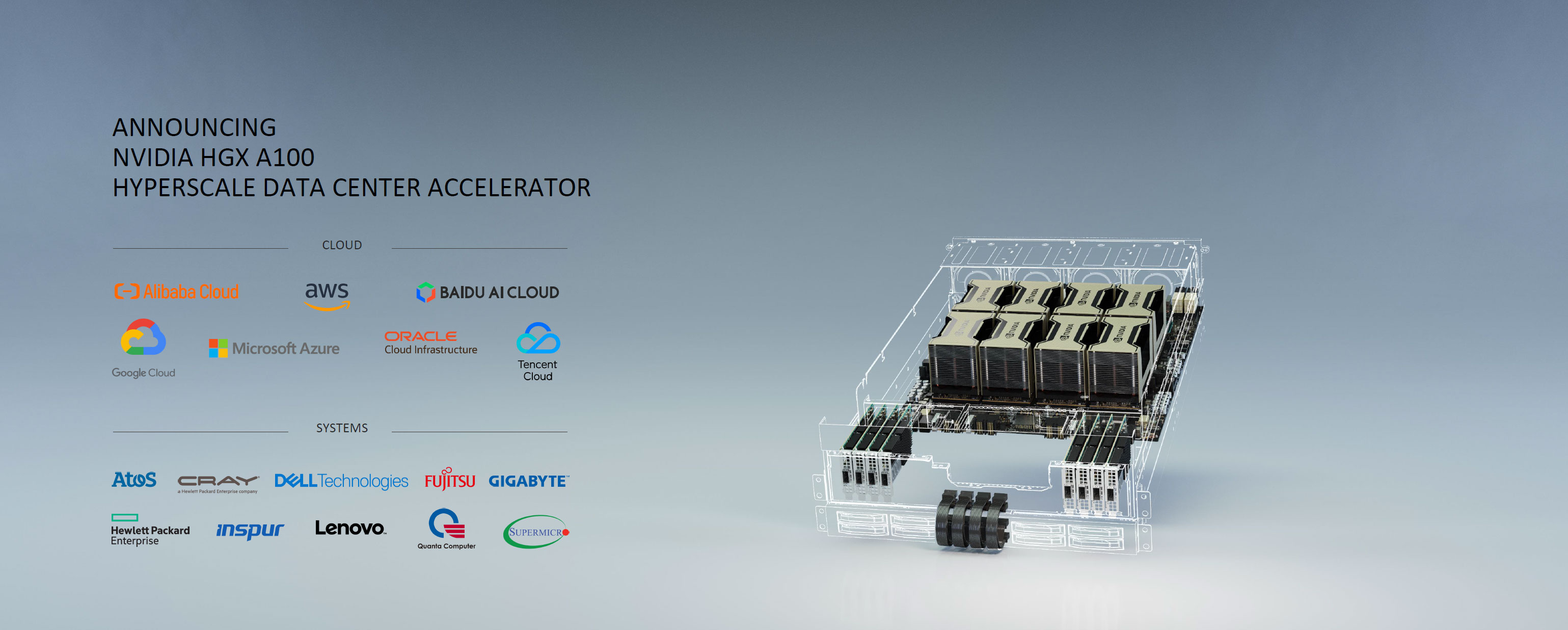
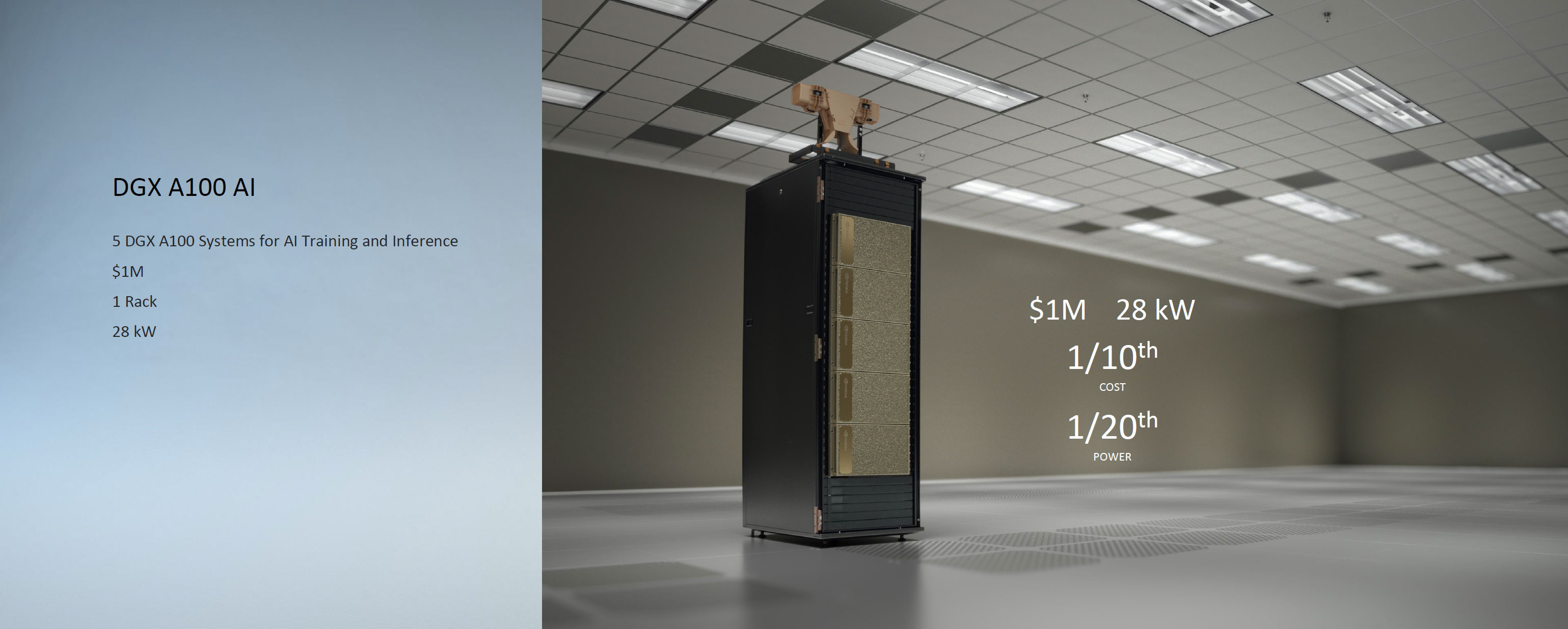
Of course, supercomputers wouldn't just want a single A100 card, and while those will exist (for inference and instancing applications, among others), the real power comes in the form of the new Nvidia DGX A100. Packing eight A100 GPUs linked via six NVSwitch with 4.8 TBps of bi-directional bandwidth, it can in effect behave as a single massive GPU with the right workloads. The eight GPUs can also provide 10 POPS (PetaOPS) of INT8 performance, 5 PFLOPS of FP16, 2.5 TFLOPS of TF32, and 156 TFLOPS of FP64 in a single node. And all this can be yours, for only $199,000—well, it could be at some point, as the waiting list is probably already quite long.
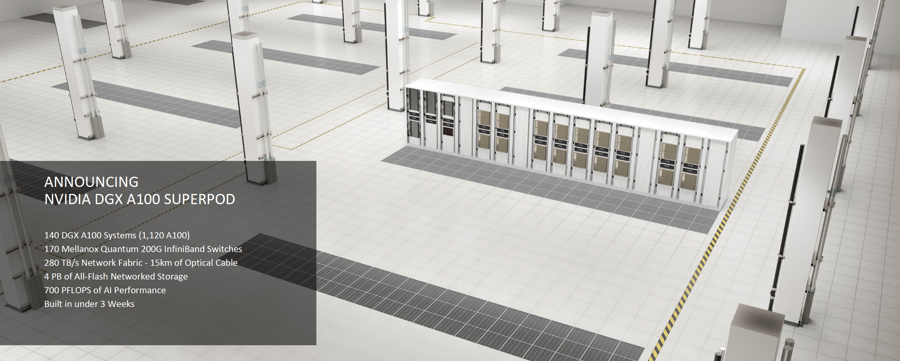
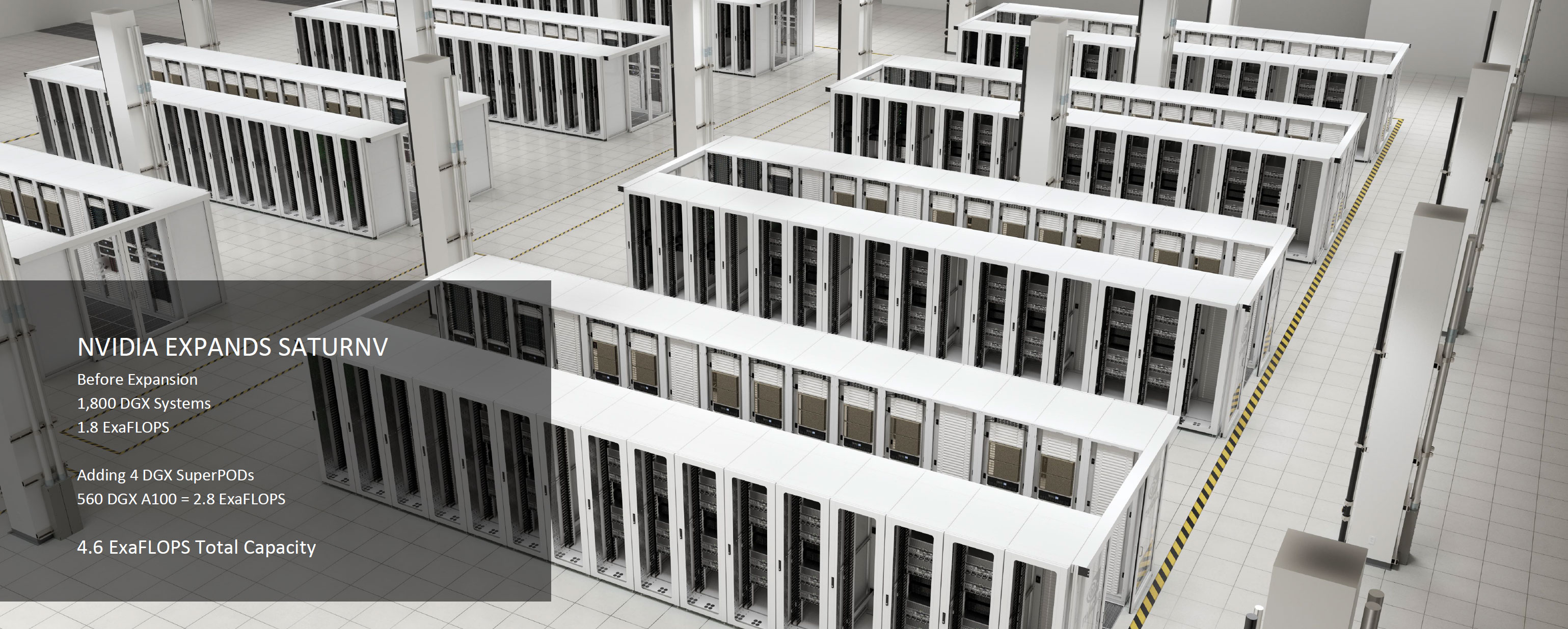
Need even more performance? Say hello to the Nvidia DGX A100 Superpod. Housing 140 DGX A100 systems, each with eight A100 GPUs (1,120 total A100 GPUs), the A100 Superpod was built in under three weeks and delivers 700 PFLOPS of AI performance. Nvidia has added four such superpods to its Saturn V supercomputer, which previously had 1,800 DGX-1 systems with 1.8 ExaFLOPS of compute. Adding just 560 DGX A100 systems tacks on another 2.8 ExaFLOPS, for a total of 4.6 ExaFLOPS.
All of this is great news for supercomputer and HPC use, but it leaves us with very little information about Nvidia's next generation Ampere GPUs for consumer cards. We know that Nvidia crammed in 2.5 times as many transistors in roughly the same die space, which means it could certainly do the same for consumer GPUs. Remove some of the FP64 and deep learning functionality and focus on ray tracing and graphics cores, and the resulting GPU should be very potent. We'll find out just how potent in the coming days.
You can view all eight parts of Jensen's keynote here:
Part 1 - Nvidia GTC keynote, introduction to data center computing
Part 2 - Nvidia GTC keynote on RTX graphics and DLSS, and Omniverse
Part 3 - Nvidia GTC keynote on GPU accelerated Spark 3.0
Part 4 - Nvidia GTC keynote on Merlin and recommender system
Part 5 - Nvidia GTC keynote on Jarvis and conversational AI
Part 6 - Nvidia GTC keynote on the A100 and Ampere architecture (yeah, this is the one you want)
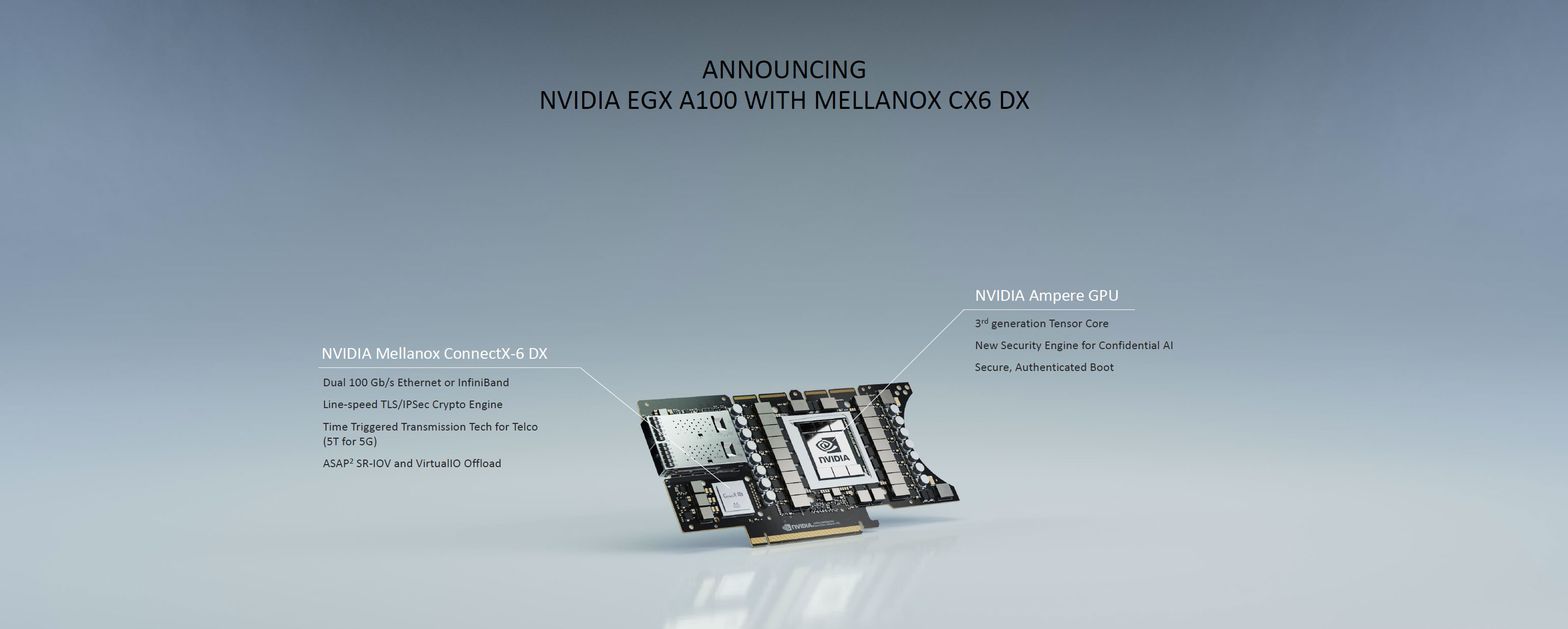
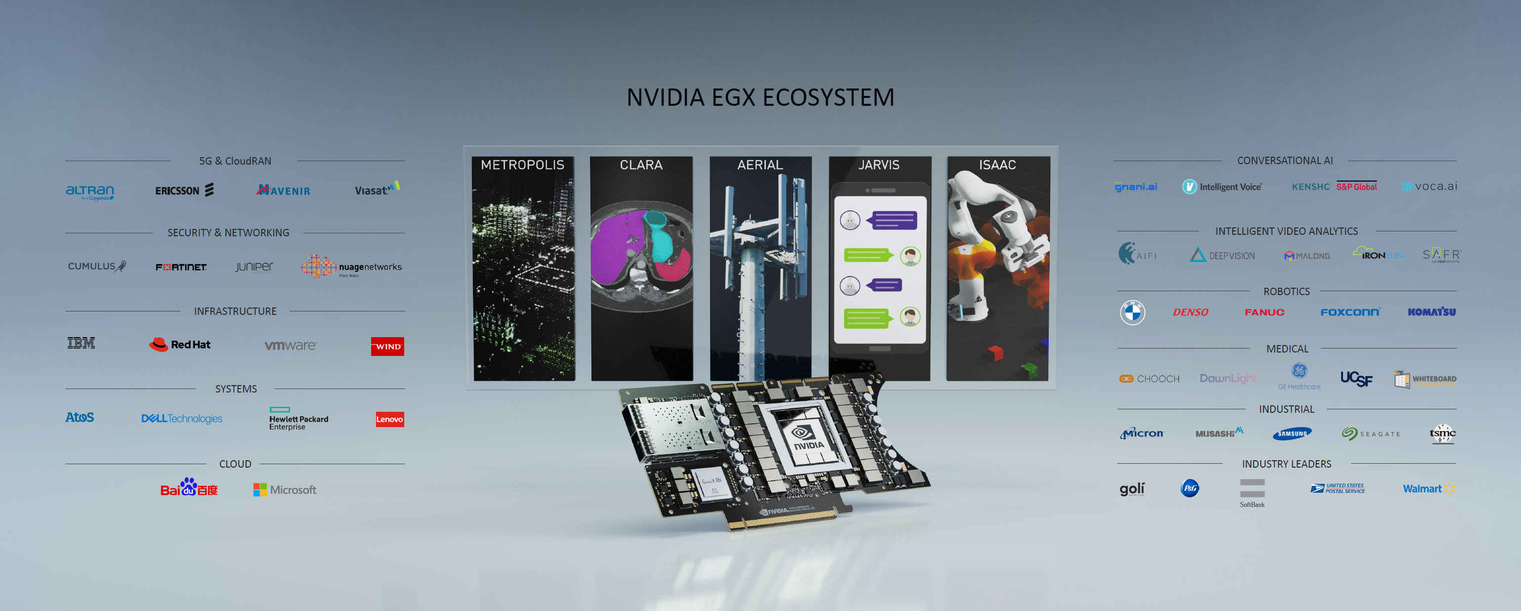
Part 7 - Nvidia GTC keynote on EGX A100 and Isaac robotics platform
Part 8 - Nvidia GTC keynote on Orin and autonomous vehicles
Part 9 - Nvidia GTC keynote conclusion




Jarred Walton is a senior editor at Tom's Hardware focusing on everything GPU. He has been working as a tech journalist since 2004, writing for AnandTech, Maximum PC, and PC Gamer. From the first S3 Virge '3D decelerators' to today's GPUs, Jarred keeps up with all the latest graphics trends and is the one to ask about game performance.
-
bit_user @JarredWaltonGPU , thanks for the coverage, as always.Reply
...but,
For workloads that use TF32, the A100 can provide 312 TFLOPS of compute power in a single chip. That's up to 20X faster than the V100's 15.7 TFLOPS of FP32 performance, but that's not an entirely fair comparison since TF32 isn't quite the same as FP32.
Right, a better comparison would be with the V100's fp16 tensor TFLOPS. Comparing it with general-purpose FP32 TFLOPS is apples vs. oranges, whereas TF32 vs fp16 tensor TFLOPS is maybe apples vs. pears.
Nvidia says elsewhere that the third generation Tensor cores support FP64, which is where the 2.5X increase in performance comes from, but details are a scarce. Assuming the FP64 figure allows similar scaling as previous Nvidia GPUs, the A100 will have twice the FP32 throughput and four times the FP16 performance
Um... don't assume that! Tensor cores are very specialized and support only a few, specific operations. You want to look at their spec for general-purpose fp64 TFLOPS.
It seems likely the A100 will follow a similar path and leave RT cores for other Ampere GPUs.
Agreed. Ray tracing is a different market segment. Even talking about photorealistic rendering for movies and such, it would make sense for them to take a page out of the Turing playbook and use the gaming GPUs for that.
the A100 can be has multi-GPU instancing that allows it to be partitioned into seven separate instances.
rats. You almost said "can has". I'd have enjoyed that.
; ) -
bit_user Reply
I think the bigger problems to solve are going to be power and cooling.InvalidError said:One step closer to building the Jupiter Brain!
On a related note, I'm reading it burns 400 W! -
JarredWaltonGPU Reply
Nvidia has posted additional details, which I'm currently parsing and updating the article. There's a LOT to digest this morning!bit_user said:@JarredWaltonGPU , thanks for the coverage, as always.
...but,
Right, a better comparison would be with the V100's fp16 tensor TFLOPS. Comparing it with general-purpose FP32 TFLOPS is apples vs. oranges, whereas TF32 vs fp16 tensor TFLOPS is maybe apples vs. pears.
Um... don't assume that! Tensor cores are very specialized and support only a few, specific operations. You want to look at their spec for general-purpose fp64 TFLOPS.
Agreed. Ray tracing is a different market segment. Even talking about photorealistic rendering for movies and such, it would make sense for them to take a page out of the Turing playbook and use the gaming GPUs for that.
rats. You almost said "can has". I'd have enjoyed that.
; ) -
JarredWaltonGPU Reply
Yes. Official specs were posted after the initial writeup, so I've fixed some things and added more details. RT cores and RTX are definitely not present.bit_user said:I think the bigger problems to solve are going to be power and cooling.
On a related note, I'm reading it burns 400 W! -
jeremyj_83 @JarredWaltonGPUReply
Isn't ECC a native feature on HBM2? If so then why would you need those extra stacks if not for redundancy? -
JarredWaltonGPU Reply
I'm not positive on this, but ECC is an optional feature for HBM2 I think. I've found reports saying Samsung's chips have it... but is it always on? That's unclear. I have to think the sixth chip is simply for redundancy, which is still pretty nuts. Like, yields are so bad that we're going to stuff on six HBM2 stacks and hope the interfaces and everything else for at least five of them work properly? I asked for clarification on the six stacks -- TWICE -- but my question somehow got missed.jeremyj_83 said:@JarredWaltonGPUIsn't ECC a native feature on HBM2? If so then why would you need those extra stacks if not for redundancy? -
jeremyj_83 Reply
"And, of course, as a native feature of HBM2, it offers ECC memory protection."JarredWaltonGPU said:I'm not positive on this, but ECC is an optional feature for HBM2 I think. I've found reports saying Samsung's chips have it... but is it always on? That's unclear. I have to think the sixth chip is simply for redundancy, which is still pretty nuts. Like, yields are so bad that we're going to stuff on six HBM2 stacks and hope the interfaces and everything else for at least five of them work properly? I asked for clarification on the six stacks -- TWICE -- but my question somehow got missed.
https://www.anandtech.com/show/15777/amd-reveals-radeon-pro-vii (bottom of the 6th paragraph)
I just remembered where I had read the ECC reference to HMB2.
Crazy idea but instead of redundancy could they use a stack as a large L3/4 cache of some sorts?
