Nvidia Ampere A100 Takes Fastest GPU Crown in First Benchmark Result

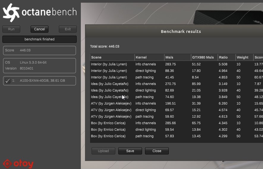
Nvidia's Ampere A100 GPU has been out since May, but we had no idea of how it performed until today. Jules Urbach, founder and CEO of OTOY, has tweeted what seems to be the first benchmark of the A100.
The A100 scored 446 points on OctaneBench, thus claiming the title of fastest GPU to ever grace the benchmark. The Nvidia Titan V was the previous record holder with an average score of 401 points. The A100 delivered up to 11.2% higher performance than the Titan V. Urbach highlighted that the A100 run was with RTX disabled.
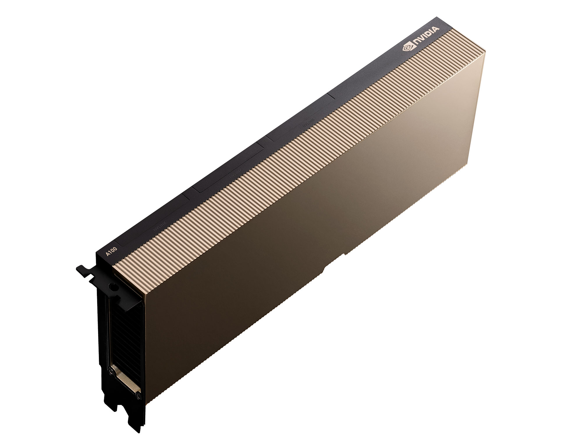
It doesn't come as a complete shock that the A100 would topple the Titan V if you look closely at the A100's composition. The GA100 silicon measures 826 millimeters-squared and flaunts 54.2 billion transistors, which is possible, thanks to TSMC's 7nm FinFET manufacturing process. The silicon comes equipped with 128 streaming multiprocessors (SMs), amounting to 8,192 CUDA cores. The A100 doesn't leverage the full die, but its specifications are impressive nonetheless.
The A100 is equipped with 6,912 CUDA cores and 432 Tensor cores. The GPU's other imposing traits include 40GB of HBM2E memory across a 5,120-bit memory interface for a bandwidth up to a whopping 1,555 GBps. The Titan V's 5,120 CUDA cores and 12GB of HBM2 memory look paltry beside the A100.
OctaneBench benchmarks graphics cards with the OctaneRender, and one of its requirements is Nvidia CUDA. Therefore, you won't find any Radeon GPUs from the Red Team on the leaderboard. You will find a generous lot of GeForce, Quadro and Tesla devices on the list though.
The GeForce RTX 2080 Ti ranks 14 on the OctaneBench leaderboard with an average score of 302. The A100 is up to 47.7% faster. Keep in mind that GA100 silicon is tailored for Nvidia's data center products. It's delusional to think it will make its way to Nvidia's forthcoming consumer graphics cards, presumably dubbed RTX 3080 and RTX 3090. The A100 is the successor to the GV100 (Volta), so it could end up in a Titan GPU.
Multiple rumors claim that mainstream Ampere graphics cards may employ the GA102 die. Obviously, it'll be smaller in comparison to the GA100 and ultimately features less SMs. Thus far, the GA102 die is rumored to have up to 84 SMs that results in 5,376 CUDA cores. This might be the silicon that Nvidia uses for the GeForce RTX 3080 Ti or GeForce RTX 3090. In any event, it's unlikely that the GA102 will outperform the GA100 given the CUDA core deficit. It could be a close fight if Nvidia gives the GA102-based GPUs some crazy clock speeds.
Get Tom's Hardware's best news and in-depth reviews, straight to your inbox.
Ampere will undoubtedly bring an important performance upgrade over Turing. There are many figures that are being thrown around, and we won't know exactly how much until Nvidia officially drops Ampere. In all likelihood, the generation-over-generation uplift will be less than 47.7%.

Zhiye Liu is a news editor, memory reviewer, and SSD tester at Tom’s Hardware. Although he loves everything that’s hardware, he has a soft spot for CPUs, GPUs, and RAM.
-
bit_user 11.2% faster than the Titan V is a pretty bad result, considering their specs.Reply
Hopefully, the disappointing improvement is simply due to some scaling issues with the benchmark. -
DoofusOfDeath ReplyThe GA100 silicon measures 826 millimeters-squared ...
That can't be right. In Imperial units, that's saying each GA100 chip is a (2.7 feet) x (2.7 feet) square. -
escksu ReplyAdmin said:The Ampere A100 has taken the Nvidia Ampere A100 Takes Fastest GPU Crown in First Benchmark Result as the fastest GPU ever benchmarked on OctaneBench.
Nvidia Ampere A100 Takes Fastest GPU Crown in First Benchmark Result : Read morebit_user said:11.2% faster than the Titan V is a pretty bad result, considering their specs.
Hopefully, the disappointing improvement is simply due to some scaling issues with the benchmark.
We have to consider the fact that A100 is designed as a compute card for specialised applications such as AI. Its not exactly a gpu, not a quadro. -
みんぱ Reply
It's more like (1.13 in) by (1.13 in). One inch squared equals 645.16 millimeters squared. One foot squared equals 92,903.04 millimeters squared. Your example of (2.7 ft) by (2.7 ft) is larger than 677,000 millimeters squared (which is 820 times GA100's die area as stated in the article). Be educated.DoofusOfDeath said:That can't be right. In Imperial units, that's saying each GA100 chip is a (2.7 feet) x (2.7 feet) square. -
bit_user Reply
I'm not familiar with the benchmark, but I got the impression it merely uses CUDA for computation. In that sense, the specs should be entirely predictive of the resultant performance.escksu said:We have to consider the fact that A100 is designed as a compute card for specialised applications such as AI. Its not exactly a gpu, not a quadro.
The Titan V has 653 GB/sec of memory bandwidth and 14.9 TFLOPS of fp32 compute (at boost clocks).
The A100 has 1555 GB/sec of memory bandwidth and 19.5 TFLOPS of fp32 compute (at ??? clocks).
So, if the workload is compute-limited, then it should be at least 30.9% faster (possibly more, depending on whether the A100 figures I saw were base or boost). However, if it's limited by memory bandwidth, then it should be 138% faster! Either way, 11.2% is really disappointing. I think it likely points to bottlenecks in the software, but we don't really know. It's definitely not good news - that's for sure! -
DonGato Reply
Thats some silly math take the square root of that to get the dimensions so 28mmX28mm die size. so now when you see a square mm or cubic mm you take the square root or cube root on a calculator to see what each side is.DoofusOfDeath said:That can't be right. In Imperial units, that's saying each GA100 chip is a (2.7 feet) x (2.7 feet) square. -
Camikazi I get that this will almost definitely be faster than the competing Radeon but come on now, Fastest GPU Crown in a benchmark that only benchmarks Nvidia GPUs...Reply -
astidcrisse ReplyDoofusOfDeath said:That can't be right. In Imperial units, that's saying each GA100 chip is a (2.7 feet) x (2.7 feet) square.
According to your math, that would make a 677 329mm square chip
I think you're missing what "square" means -
bit_user Reply
I believe the main point of the article was to infer how much faster the gaming variants of Ampere GPUs could be than their Turing counterparts. However, the analysis is clearly problematic, for a number of reasons.Camikazi said:I get that this will almost definitely be faster than the competing Radeon but come on now, Fastest GPU Crown in a benchmark that only benchmarks Nvidia GPUs...
