SiFive Tapes Out First 5nm TSMC RISC-V Chip With 7.2 Gbps HBM3
SiFive and OpenFive hit 5nm milestone.

SiFive on Tuesday said that that its OpenFive division has successfully taped out the company's first system-on-chip (SoC) on TSMC's N5 process technology. The SoC can be used for AI and HPC applications and can be further customized by SiFive customers to meet their needs. Meanwhile, elements from this SoC can be licensed and used for other N5 designs without any significant effort.
The SoC contains the SiFive E76 32-bit CPU core(s) for AI, microcontrollers, edge-computing, and other relatively simplistic applications that do not require full precision. It uses OpenFive's D2D (die-to-die) interface for 2.5D packages as well as OpenFive's High Bandwidth Memory (HBM3) IP subsystem, which includes a controller and PHY that supports data transfer rates of up to 7.2 Gbps.
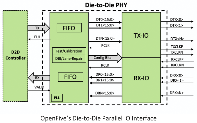
The announcement represents a milestone for SiFive and OpenFive, as the SoC is the first RISC-V-based device to be made using a 5nm node. Meanwhile, the announcement also contains two interesting facts. The first one is of course OpenFive's implementation of an HBM3 solution and its rather bold data transfer rate expectation (2X compared to the fastest HBM2E available today). The second one is OpenFive's D2D interface for chiplets that uses 16 Gbps NRZ signals with clock forwarding architecture, comprised of 40 IOs per channel, and provides throughput of up to ~1.75Tbps/mm.
Article continues belowThe current design will hardly ever be used 'as is', but parties interested in building a high-performance 5nm RISC-V SoC for AI or HPC applications can take it as a the base design and equip it with their own or third-party IP (e.g., custom accelerators, high-performance FP64-capable cores, etc.).
Alternatively, all three key components of the SoC implemented using TSMC's N5 node — the E76 core, the D2D interface and its physical implementation (which includes built-in PLL, programmable output drivers, and link training state machines), and the HBM3 memory solution (controller, I/O, PHY) — can be licensed separately.
The tape out means that the documentation for the chip has been submitted for manufacturing to TSMC, which essentially means that the SoC has been successfully simulated. The silicon is expected to be obtained in Q2 2021.
Get Tom's Hardware's best news and in-depth reviews, straight to your inbox.

Anton Shilov is a contributing writer at Tom’s Hardware. Over the past couple of decades, he has covered everything from CPUs and GPUs to supercomputers and from modern process technologies and latest fab tools to high-tech industry trends.
-
InvalidError Reply
As long as we are still talking about one-bit-per-baud busses, the two are fundamentally interchangeable: each data pin of a 7.2GT/s bus is carrying 7.2Gbps.Kamen Rider Blade said:When they stated 7.2 Gbps, did they really mean 7.2 GT/s instead? -
Kamen Rider Blade Reply
While that may be true, shouldn't we try to use the correct unit to represent what's being transferred instead of the more common colloquialism?InvalidError said:As long as we are still talking about one-bit-per-baud busses, the two are fundamentally interchangeable: each data pin of a 7.2GT/s bus is carrying 7.2Gbps.
This way, moving foreward, more people will start to understand the difference! -
InvalidError Reply
Using Gbps is pretty standard for chip manufacturers describing the bandwidth-per-pin/lane density of their interfaces.Kamen Rider Blade said:While that may be true, shouldn't we try to use the correct unit to represent what's being transferred instead of the more common colloquialism?
GT/s will become awkward when more devices start using PAM4 and higher signaling like GDDR6X has. What is the GT/s rate of 19Gbps GDDR6X? Hint: the correct answer is not 19GT/s since GDDR6X uses PAM4 (2bits/baud) signaling. -
lazyabum If RISC-V becomes the new king of of raspberry pi, a decade of development will be stretched two decades more.Reply
