Samsung Plans to Adopt 1.4nm Process Tech by 2027
Samsung outlines plans for 2nm, 1.4nm production nodes.

Samsung Foundry this week outlined its longer-term roadmap covering its next-generation fabrication processes as well as expansion of its production capacities. The company has no plans of slowing down development and deploying new manufacturing technologies as well as expanding its manufacturing capacities to meet demand for advanced chips going forward.
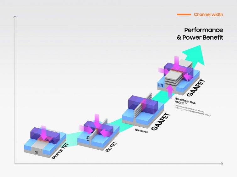
Samsung Foundry intends to start making chips using its next-generation 2nm fabrication process by 2025 as well as its 1.4nm production node by 2027, according to a report by Nikkei. Earlier this year Samsung began to make semiconductors using its first-generation 3nm manufacturing technology (also known as 3GAE, or gate-all-around early). In 2024 the company will adopt its second-generation 3nm node (also known as 3GAP, or gate-all-around plus).
Because it is getting harder to develop new fabrication processes and adopt them for mass production, it is not particularly surprising that Samsung's 2nm (or 20 angstroms) node will be ready in about two years. By the time Samsung Foundry will be ready with its 2nm technology, its rival Intel will start using its 20A node in mid-2024 and 18A node in mid-2025, according to the current roadmap. Meanwhile, Taiwan Semiconductor Manufacturing Co. plans to kick of high-volume production using its 2nm node in the second half of 2025 and deliver the first chips in early 2026.
In recent years Samsung invested heavily in new fabs in a bid to produce more advanced system-on-chips for its Samsung Foundry clients as well as sophisticated 3D NAND and DRAM chips. For several years the company spent more money on advanced semiconductor production capacities than almost anyone in the industry — and it apparently has no plans to slow investments.
Samsung intends to triple its advanced chips production capacity by 2027, according to a Reuters report citing officials from the company. Samsung did not disclose exact targets and what it considered advanced production capacity, though it is certain that the company will continue to invest in new semiconductor capacities.
Samsung needs to make leading-edge chips not only for its fabless clients, but also for its own products, including consumer electronics automotive applications, 5G and 6G connectivity, and other products.
To meet demand for its own- and third-party chips, Samsung is building its new all-new fabs near Taylor, Texas, and is planning to expand its production capacities in South Korea. The fab in Texas is expected to begin high volume manufacturing in 2024 using one of the company's 3nm-class nodes, according to a report from Bloomberg citing officials from the company.
Get Tom's Hardware's best news and in-depth reviews, straight to your inbox.

Anton Shilov is a contributing writer at Tom’s Hardware. Over the past couple of decades, he has covered everything from CPUs and GPUs to supercomputers and from modern process technologies and latest fab tools to high-tech industry trends.
-
PiranhaTech Angstrom or picometer is making a lot of sense. I do lean more towards pm though. We had triple digit nm (ex: 800nm) before.Reply -
Kamen Rider Blade Once we're < 1 nm, we'll be going to single-digit Angstroms.Reply
1 Nanometer = 10 Ångstroms
Ergo 9 Angstroms down to 1 Angstrom
Once we go < 1 Angstrom, we'll be going to double-digit Picometers
1 Ångstrom = 100 pm
ergo 99 pm to 1 pm
