TSMC Preps for 3nm Risk Production
TSMC confident in semiconductor demand, economy recovery.
Get Tom's Hardware's best news and in-depth reviews, straight to your inbox.
You are now subscribed
Your newsletter sign-up was successful
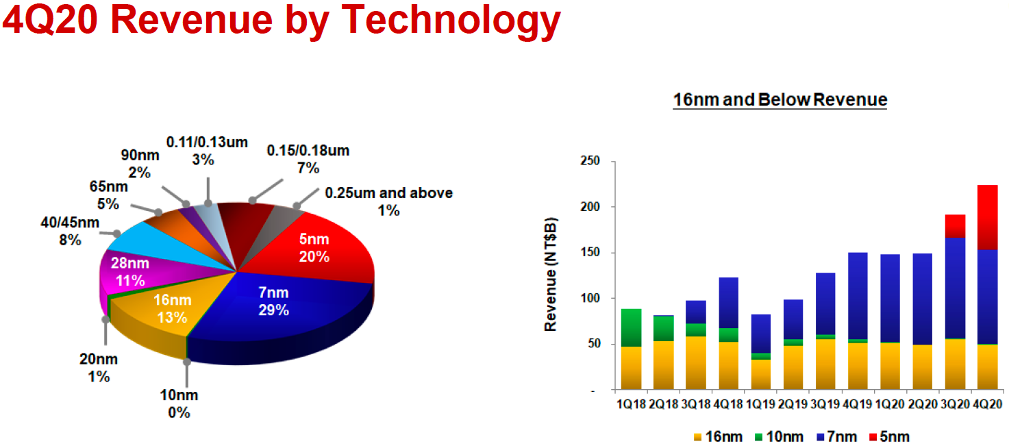
Taiwan Semiconductor Manufacturing Co. said this week that it would significantly increase its capital expenditures this year as it needs to build and equip new fabs to ramp up its existing and next-generation leading-edge process technologies. Demand for advanced fabrication nodes is on the rise. In Q4 2020, revenue for N5 (5 nm) and N7 (7 nm) technologies accounted for nearly half of TSMC's revenue, so it makes a great sense for the manufacturer to continue investing in leading-edge capacities. Furthermore, as Apple and Intel plan to increase orders to TSMC, the foundry will also need more capacity.
TSMC to Spend Up to $28 Billion on Production Facilities in 2021
TSMC's management plans to spend from $25 billion to $28 billion on capital expenditures in 2021, the world's largest contract maker of semiconductor announced this week.
If TSMC's board approves all the investments proposed by the management, then TSMC's CapEx will rise by 45% ~ 62% year-over-year from $17.2 billion in 2020. The lion's share of TSMC's capital budget will be spent on expanding production capacities for the company's N5 and N7 nodes as well as equipping a leading-edge fab for its N3 (3 nm) node that will be used starting from the second half of 2022.
Article continues below"Out of the $25 to $28 billion CapEx for 2021, about 80% of the capital budget will be allocated for advanced process technologies, including 3 nm, 5 nm and 7 nm," said Wendell Huang, chief financial officer at TSMC, during this week's earnings call with analysts and investors. "About 10% will be spent for advanced packaging and mask making and about 10% will be spent for speciality technologies."
"The 2021 CapEx is largely for N5 expansion (at least 2x its current 55-60k WPM capacity), and N3 build is limited to pilot line/initial production (+10-15k WPM, though we expect N3’s capacity to be similar to N5’s upon full ramp-up)," Szeho Ng, an analyst with China Renaissance Securities, wrote in a note to clients on Friday.
Production of semiconductors is an extremely capital-intensive business and as process technologies get more advanced and manufacturing tools get more expensive, chipmakers have to increase their CapEx budgets to build fabs that cost as much as $20 billion or even more. Because of increasingly high R&D and fab costs, numerous contract makers of semiconductors had to pull out from the leading-edge and focus on specialized technologies in the recent years.
N5 & N7 Accounted for 49% of TSMC's Revenue in Q4 2020
But with a number of rivals out of the game, TSMC now has more clients than ever. And considering the fact that there are a number of ongoing megatrends — such as 5G, AI, high-performance computing (HPC), and edge computing — that require advanced chips produced using the most sophisticated technologies possible, demand for TSMC's higher-end production services is on the rise today and will continue growing in the coming years.
Get Tom's Hardware's best news and in-depth reviews, straight to your inbox.
In the fourth quarter, sales of wafers processed using N5 accounted for 20% of TSMC's total wafer revenue, whereas sales of N7 and 12 nm/16 nm accounted for 29% and 13% respectively. In general, leading-edge N5 and N7 nodes commanded 49% of TSMC's wafer revenue, whereas advanced nodes (N5, N7, N12/N16) accounted for 62% of the company's total wafer revenue.
TSMC's N5 process technology in Q4 2020 was primarily used by Apple, which uses it for its A14 system-on-chips for smartphones and tablets as well as M1 SoCs for its latest PCs. The company's N7 is used more widely by companies like AMD, Apple, Nvidia, Qualcomm, and Xilinx, whereas N12/N16 is used by dozens of companies for all kinds of applications.
"Our fourth quarter business was supported by strong demand for our industry-leading 5 nm technology, driven by 5G smartphone launches and HPC-related applications," said Mr. Huang. "Moving into first quarter 2021, we expect our business to be supported by HPC-related demand, recovery in the automotive segment, and a milder smartphone seasonality than in recent years."
TSMC's N5 is a major improvement over N7 node that enables a 15% higher performance (at the same power and complexity) or a 30% lower power consumption (at the same frequency and complexity), and an up to 1.8X higher transistor density (not for all structures). In addition, N5 uses extreme ultraviolet (EUV) lithography on more than 10 layers to reduce mask count to 81 as well as reduce or even avoid usage of multipatterning, which optimizes yields and costs. Considering all the advantages that N5 has over N7, the majority of TSMC's clients that use N7 now will migrate to N5 over time.
Later this year TSMC will offer its customers a performance-enhanced version of N5 that is called N5P. The latter is projected to enable a 5% performance gain and/or a 10% power reduction over N5 while staying generally compatible. Yet, N5P will be used by select chip designers only as next year TSMC will offer N4 that will provide further PPA (power, performance, area) enhancements while being compatible with N5 on design rules, IPs, and SPICE levels. TSMC's fabs that currently process wafers using its N5 technology will also be able to use N5P as well as N4, so any investments going there will be used for years.
N3 Could Be More Successful Than N5 and N7
TSMC's next major step after N5 will be N3 (3 nm). This technology promises an up to 15% performance gain (at the same power and transistor count), or an up to 30% power reduction (at the same speed and transistor count), along with an up to 20% higher SRAM density as well as an up to 70% higher logic density. This technology is still in development and will be used starting from the second half of 2022.
TSMC says that it sees more interest in N3 from potential clients in the HPC (TSMC considers 'HPC' all CPUs, GPUs, FPGAs, non-mobile SoCs, special-purpose accelerators, etc.) and smartphone spaces than it did with N5 and N7 when they were at a similar stage of development.
"We are seeing a much higher level of customer engagement for both HPC and smartphone application at N3 as compared with N5 and N7 at a similar stage," said C. C. Wei, Chief Executive Officer of TSMC. "Risk production is scheduled in 2021, and volume production is targeted in the second half of 2022."
TSMC does not disclose any actual numbers that would quantify interest for N3 from its clients, but since many new applications are going to emerge in the coming years, it is not surprising that more players with more designs will be opting for a leading-edge process technology in 2022 ~ 2025 than they did several years ago. Furthermore, since N3 continues to rely on FinFET transistor structures with predictable performance and costs, the fabrication process will be a very long node as its successors will move to GAAFETs (gate-all-around field effect transistors), which is going to have a significant impact on design costs. For example, TSMC's 28 nm node that relies on planar transistors accounted for 11% of its wafer revenue in Q4 2020, nine years after the fabrication process was introduced.
"We note the bold expansion reflects N3-5 as long- lasting big nodes with expected robust future demand beyond the initial wave from key clients," Szeho Ng, an analyst with China Renaissance Securities, wrote in a note to clients on Friday.
While eventually dozens of companies will use TSMC's N3 and N5, there are two customers that are going to have a significant impact on TSMC's CapEx budgets in the coming years: Apple and Intel.
Apple: More Chips Needed
Traditionally, the bulk of Apple's orders to TSMC have been its SoCs for smartphones and tablets. Many of its suppliers produce their chips at TSMC as well, but those semiconductors are not made under Apple's orders and are not made exclusively for the company. As Apple transits its PCs to its own SoCs, starts to use its own modems inside its smartphones and tablets, and increases sales of its accessories that rely on its own system-in-packages (SiPs), it will significantly increase its orders to TSMC.
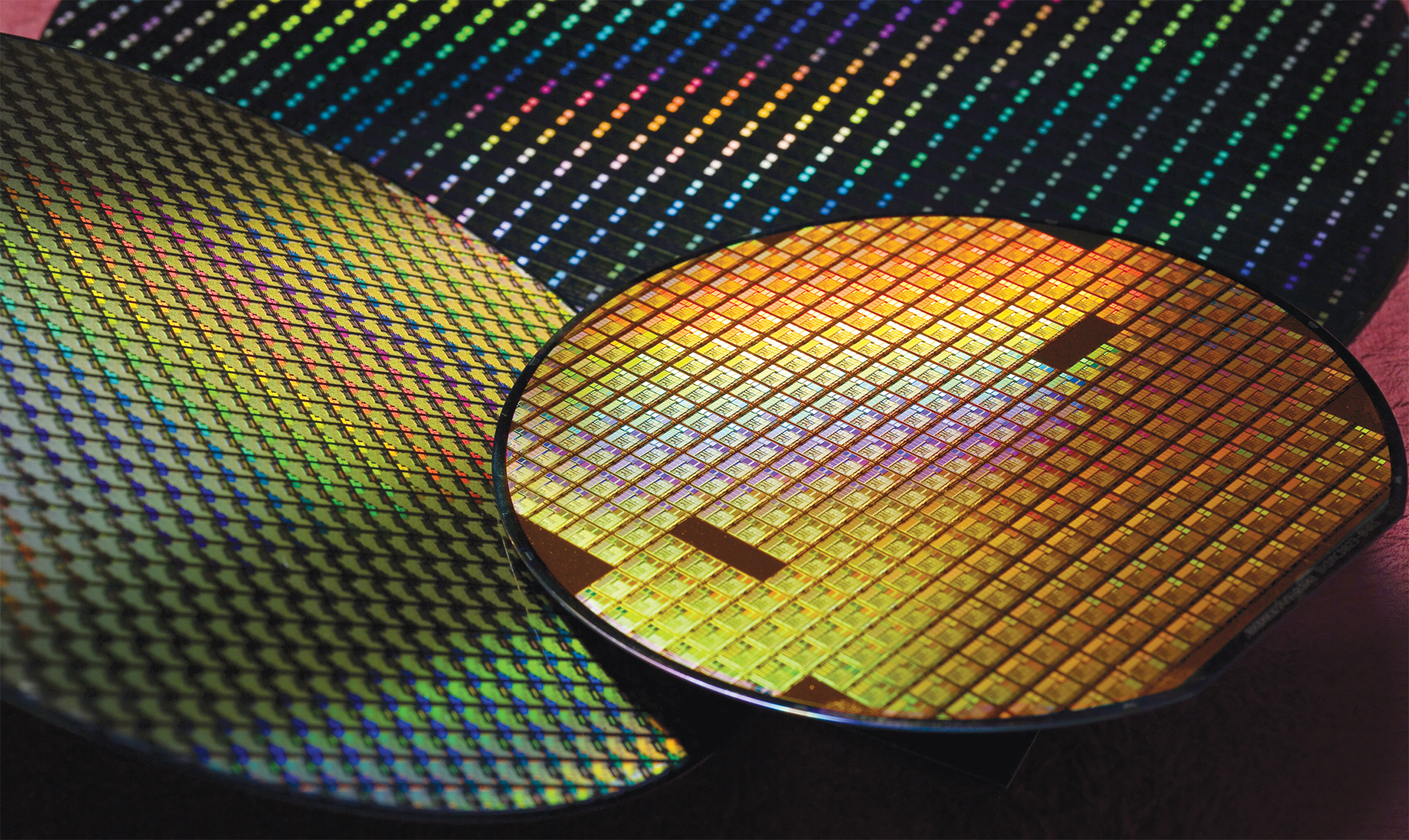
Apple is the world's No. 4 PC supplier that shipped 23.102 million computers last year and commanded about 7.6% of the PC market. Sales of PCs in 2020 totalled 302.6 million units, according to IDC. Once the technology giant completes transition of Macs from Intel CPUs to its Apple Silicon SoCs, it will need at least 23.102 million fairly big chips (the M1 is at 120 sq. mm, which is 26 sq. mm smaller compared to Intel's Tiger Lake-U) every year assuming that the market stays flat and Apple stops gaining market share (something that it has been doing for years).
Apple was also the third largest supplier of smartphones in 2019 with 191 million units shipped, based on IDC's data. When the company ceases to use third-party 5G modems (which happen to be made using a leading-edge process technology) and transits to its own, it will increase its orders to TSMC by another ~200 million of chips every year.
Apple's transitions to its PC SoCs and modems will be completed within the next couple of years. While it is hard to quantify Apple's orders to TSMC in terms of wafers today, it is safe to say that the addition of ~25 million PC SoCs and ~200 million modems to around ~200 million smartphone SoCs that TSMC produces today will significantly increase the number of wafers that the foundry processes for Apple.
Intel: A Wildcard
Intel already outsources manufacturing of multiple products to TSMC and has confirmed officially and unofficially that it would produce Atom and Xeon SoCs as well as GPUs at TSMC. What nobody knows at this point is whether Intel intends to make client and server CPUs at TSMC and if it has such plans, what percentage of its CPUs will be made at TSMC.
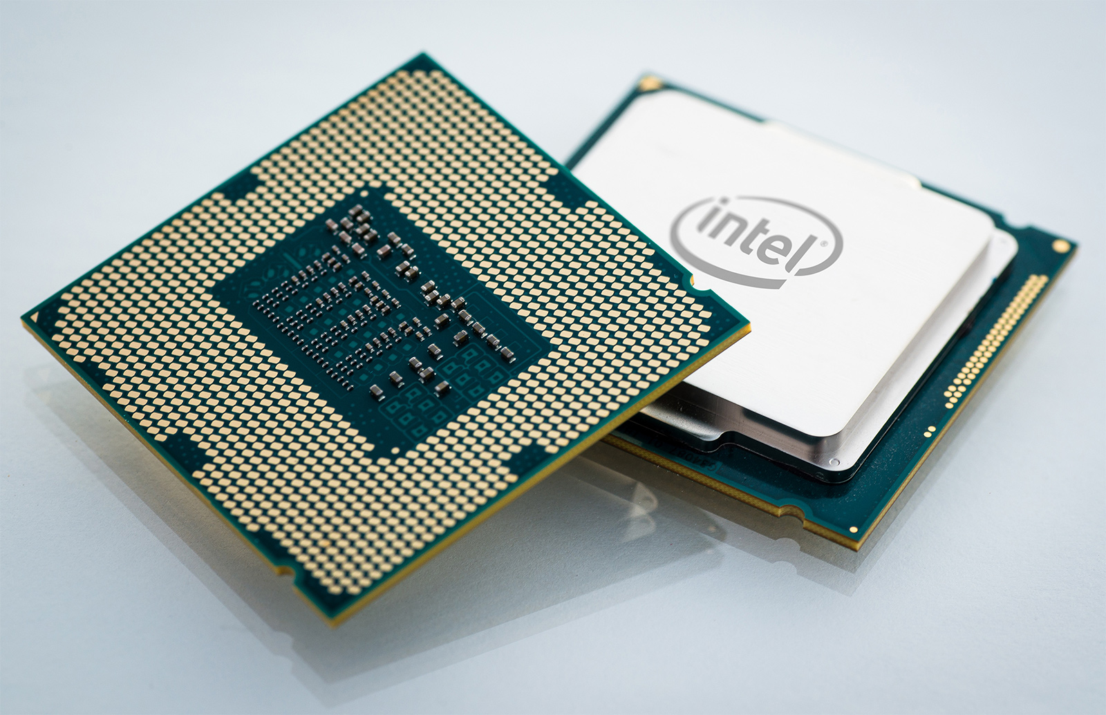
Since Intel's outsourcing plans are unclear and perhaps are even undecided, it is not good business to make too many assumptions at the moment. Yet, there are a couple of things to keep in mind. Intel sells hundreds of millions of processors and chipsets for client PCs every year and even if the company decides to outsource 10% ~ 15% of its client CPU/chipset output to TSMC, it will still be tens of millions of units added to Intel's existing orders to the foundry.
Intel traditionally uses advanced nodes, so to land its orders, which are going to be significant, TSMC will need to have enough capacity to serve the CPU giant along with other customers.
Summary
TSMC's management plans to increase its 2021 CapEx budget by 45% ~ 62% year-over-year to record $25 billion ~ $28 billion in a bid to expand its leading-edge production capacities and prepare to ramp up production using its N3 process technology in the second half of 2022.
The company sees the ongoing megatrends like 5G, artificial intelligence, high-performance computing (HPC), and edge computing as the main drivers for advanced semiconductors demand in the coming years.
Apple, which is already TSMC's main customer for advanced nodes, will likely significantly increase its orders to the foundry in the coming years as it transits to its own Apple Silicon SoCs for PCs and in-house designed modems, which will further drive demand for TSMC's leading-edge manufacturing technologies.
Intel is also going to outsource more of its products to TSMC in the coming years, which will be another factor that will increase demand for the foundry's sophisticated fabrication processes.

Anton Shilov is a contributing writer at Tom’s Hardware. Over the past couple of decades, he has covered everything from CPUs and GPUs to supercomputers and from modern process technologies and latest fab tools to high-tech industry trends.
-
jkflipflop98 They're basically saying that they think they know how to build the layers, and they're going to start trying to run some wafers through the entire process line.Reply -
Uniblab Reply
Seriously suprised that intel has fallen behind as they were process node leading up until they hit some kind of barrier around 10nm. 3nm is where <if I remember correctly>, is where the actual atomic structure becomes a barrier. Cant logically make a transistor smaller than the atom itself. Or can they? I am still suprised that it takes soo much to go soo small and as far as I know there is only one fab machine manufacturer that is making the machines that can go so small. Deep UV is only made by ASML, so that kinda restricts it to the fabs that are already capable to accept the tooling. New Fab? 100 million per toolset? Wonder how long before TSMC will have any appreciable competition in that field. If intel is laying behind the bushes - I dont think they make their own tooling - only TSMC will be able to go so small. The booming business of making things smaller.jkflipflop98 said:They're basically saying that they think they know how to build the layers, and they're going to start trying to run some wafers through the entire process line. -
spongiemaster Reply
Here's a link which explains it in a bit more detail.Co BIY said:Very interesting article.
Please define "Risk Production" for those of us less savvy.
https://www.edn.com/tsmc-risk-production-what-does-it-mean-for-28nm/
Uniblab said:3nm is where <if I remember correctly>, is where the actual atomic structure becomes a barrier. Cant logically make a transistor smaller than the atom itself.
3nm is just a marketing term and is not the gate length that it originally represented. The gate length of Intel's 10nm process is 18nm and Intel's 10nm is roughly equivalent to TSMC's and Samsung's 7nm in transistor density, so their labels are even further from the truth. -
jkflipflop98 ReplyUniblab said:Seriously suprised that intel has fallen behind as they were process node leading up until they hit some kind of barrier around 10nm. 3nm is where <if I remember correctly>, is where the actual atomic structure becomes a barrier. Cant logically make a transistor smaller than the atom itself. Or can they? I am still suprised that it takes soo much to go soo small and as far as I know there is only one fab machine manufacturer that is making the machines that can go so small. Deep UV is only made by ASML, so that kinda restricts it to the fabs that are already capable to accept the tooling. New Fab? 100 million per toolset? Wonder how long before TSMC will have any appreciable competition in that field. If intel is laying behind the bushes - I dont think they make their own tooling - only TSMC will be able to go so small. The booming business of making things smaller.
You have to remember, this "3nm" node isn't actually 3nm. They might be able to get a 3nm line width at the contact/M0 layer, but that's about it. 3nm is just a marketing term.
