Arrow Lake die shot shows off the details of Intel's chiplet-based design
Arrow Lake might be slow in gaming, but the architecture is still a sight to behold under the hood.
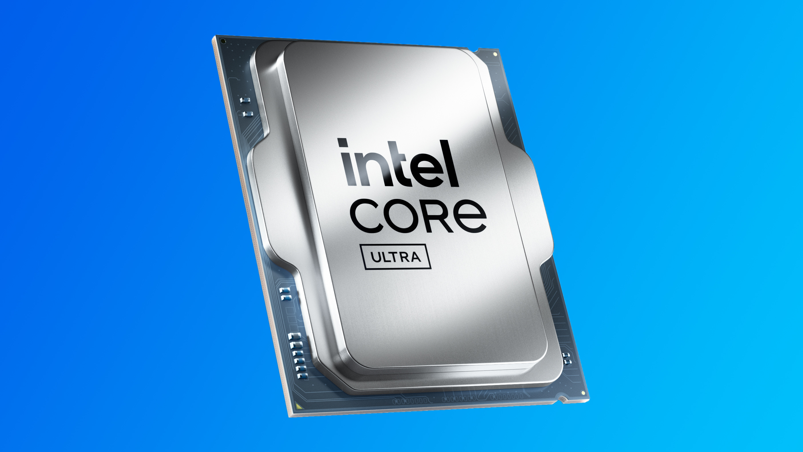
Die shots of Intel’s Arrow Lake architecture have been published, revealing Intel’s chiplet (tile) infused design in all of its glory. Andreas Schiling on X shared several images of Arrow Lake up close, revealing the layout of Arrow Lake’s individual tiles and the layout of the cores inside the compute tile.
The first photo exposes the full die of Intel’s desktop Core Ultra 200S series CPUs, with the compute tile on the upper left, the IO tile on the bottom, and the SoC tile and GPU tile on the right. To the bottom left and top right are two filler dies designed to provide structural rigidity.
A few highlights from the deep analysis of #ArrowLake by @highyieldYT pic.twitter.com/WFUG0xVaFEMay 5, 2025
The compute die is fabbed on TSMC’s bleeding-edge N3B node, with a total area of 117.241 mm². The IO tile and SoC tile are fabbed on TSMC’s older N6 node, with the IO tile measuring 24.475mm squared and the SoC tile 86.648mm squared. All of the tiles rest on an underlying base tile fabbed on Intel’s 22nm FinFET node. Arrow Lake is the first Intel architecture that is fabricated entirely using nodes from a competitor, except for the base tile.
The next image shows all of the sub-components for the secondary tiles in Arrow Lake. The I/O die houses the Thunderbolt 4 controller/display PHY, PCIe Express buffers/PHYs, and TBT4 PHYs. The SoC tile houses the display engines, media engine, more PCIe PHYs, buffers, and the DDR5 memory controllers. The GPU tile houses four Xe GPU cores and an Xe LPG (Arc Alchemist) render slice.
The final image shows off Intel’s latest core configuration for Arrow Lake, which differs from previous hybrid Intel architectures. For Arrow Lake, Intel opted to sandwich the E-cores between the P-cores rather than putting them all in their own cluster, allegedly to reduce thermal hotspots. Four of the eight P-cores reside on the borders of the die with the other four residing in the middle of the die. The four E-core clusters (which house four cores each) are sandwiched between the outer and inner P-cores.
Schilling’s die shot also exposes the cache layout for Arrow Lake, comprised of 3MB of L3 cache per P-core (36MB in total) and 3MB of L2 cache per E-core cluster, with 1.5MB shared between two cores directly. An interconnect bridges the two L2 cache clusters (and their associated cores) together, which is also responsible for connecting each core cluster to the ring agent. One major upgrade Intel made with Arrow Lake is connecting the E-core clusters to L3 cache shared by the P-cores, effectively giving the E-cores an L3 cache.
Arrow Lake is one of Intel’s most complex architectures to date and the first from the company to bring a chiplet-style design to the desktop market. That said, Intel’s first attempt at a desktop chiplet-based competitor has not been well received, due to latency issues from the interconnect, which is responsible for connecting all the tiles together. Intel is attempting to rectify the issue through firmware updates. Still, its current implementation can’t touch AMD’s competing Ryzen 9000 CPUs (such as the 9800X3D), nor is it enough to even beat its own previous-generation 14th-generation processors in gaming (such as the 14900K).
Stay On the Cutting Edge: Get the Tom's Hardware Newsletter
Get Tom's Hardware's best news and in-depth reviews, straight to your inbox.
All that said, moving to a chiplet approach will afford Intel more ways to optimize its architectures down the road, in a more efficient manner. Each tile can be developed independently of others and built with different nodes to improve yields, optimize development, and reduce production costs.

Aaron Klotz is a contributing writer for Tom’s Hardware, covering news related to computer hardware such as CPUs, and graphics cards.
-
bit_user Reply
No, it wasn't bleeding edge. Apple was already shipping M3-series SoCs on it for like 8 or 10 months, by the time it launched and was in the process of finalizing the M4-series on N3E. Intel's own Lunar Lake launched on N3B, months earlier.The article said:The compute die is fabbed on TSMC’s bleeding-edge N3B node,
It's not their first attempt. That was Meteor Lake-S, which they cancelled. There are even Meteor Lake-S engineering samples floating around, proving that they got quite far before pulling the plug on it.The article said:Intel’s first attempt at a desktop chiplet-based competitor has not been well received
The distinction isn't mere nit-picking. It means that, while they were finishing Arrow Lake, they already had an idea of what issues and challenges they would face. Maybe it was still too late to do much about them, but that's different than going in completely blind.
First, each E-core cluster has 4 MB of L2 cache. Aaron obviously just glanced at the image (missing the 1 MB slice, in the process) and not the actual specs. Otherwise, wouldn't have made that error.The article said:and 3MB of L2 cache per E-core cluster, with 1.5MB shared between two cores directly.
Second, nowhere does the original author (High Yield) ever say that the 1.5 MB slices are specifically shared between the two E-cores on either side of them. If Aaron just took a wild guess that's what was happening, he really shouldn't do that.
I'll do you a favor and link exactly the part of the vid where the author talks about the E-cores, so you can see/hear for yourself. It's pretty short (only about 16 seconds), at 13:04.
wusyYscQi0o:784View: https://youtu.be/wusyYscQi0o?t=784
Better yet, I found some evidence that the E-cores don't have preferential access to the 1.0 or 1.5 MB L2 slices adjacent to them. If they did, then there should be a corresponding bump in this graph. Instead, it's flat all the way out to 4096 kiB:
Source: https://chipsandcheese.com/p/skymont-in-desktop-form-atom-unleashed
It's also kinda weird that Aaron only linked to Andres' tweet, which was nothing more than a couple frame grabs from that Youtube video and a link to the youtuber's account. He could've just linked straight to the video and included his own frame grabs of it.
Tagging @PaulAlcorn and @JarredWaltonGPU . I hope we can see better fact-checking, in the future. -
bit_user Reply
Yeah, I've seen die shots of it that came out, before. I haven't gone back and tried to compare them, but I know it's not easy to make these photos and I think the more the merrier!DS426 said:Kind of late to build hype and excitement for Arrow Lake now. :ROFLMAO:
: D
I think I read they have to actually run the de-lidded CPU and use an infrared sensor, or else you wouldn't see much.
Edit: here, I found them.
https://www.tomshardware.com/pc-components/cpus/asus-shares-official-die-shots-of-the-core-ultra-9-285k-in-depth-annotations-break-down-intels-disaggregated-approach -
DS426 Reply
My silliness aside, I agree: the more, the merrier! :) Indeed it sounds like it's quite hard to get good die shots.bit_user said:Yeah, I've seen die shots of it that came out, before. I haven't gone back and tried to compare them, but I know it's not easy to ...
-
Eximo LGA 1366 the last time they did a one and done socket/chipset?Reply
I think LGA 775/771 had some life in it beyond the consumer chips. -
usertests All Intel desktop CPUs for the foreseeable future are going to be made of chiplets like this. Hopefully they can make some of their own next time.Reply
Is it just me, or does that Media Engine look huge? Isn't that what's handling video decode/encode? -
usertests Reply
Someone looking for power efficiency, somehow. Arrow Lake is said to be more efficient than Raptor Lake at lower TDPs.oninoshiko said:Who would ever buy a glued together chip!? /s -
Thunder64 Replyusertests said:Someone looking for power efficiency, somehow. Arrow Lake is said to be more efficient than Raptor Lake at lower TDPs.
You missed the joke. Years ago Intel said AMD was essentially inferior for using "glue". I guess this was during the Zen 2 days. -
usertests Reply
I already hit Like for the joke.Thunder64 said:You missed the joke. Years ago Intel said AMD was essentially inferior for using "glue". I guess this was during the Zen 2 days.
Sniffing the glue is obviously the root cause of the latency problems, and overall performance loss is from using less aggressive voltages than Raptor Lake.

