Asus shares official die shots of the Core Ultra 9 285K — In-depth annotations break down Intel's disaggregated approach
Experience the beauty in every detail.
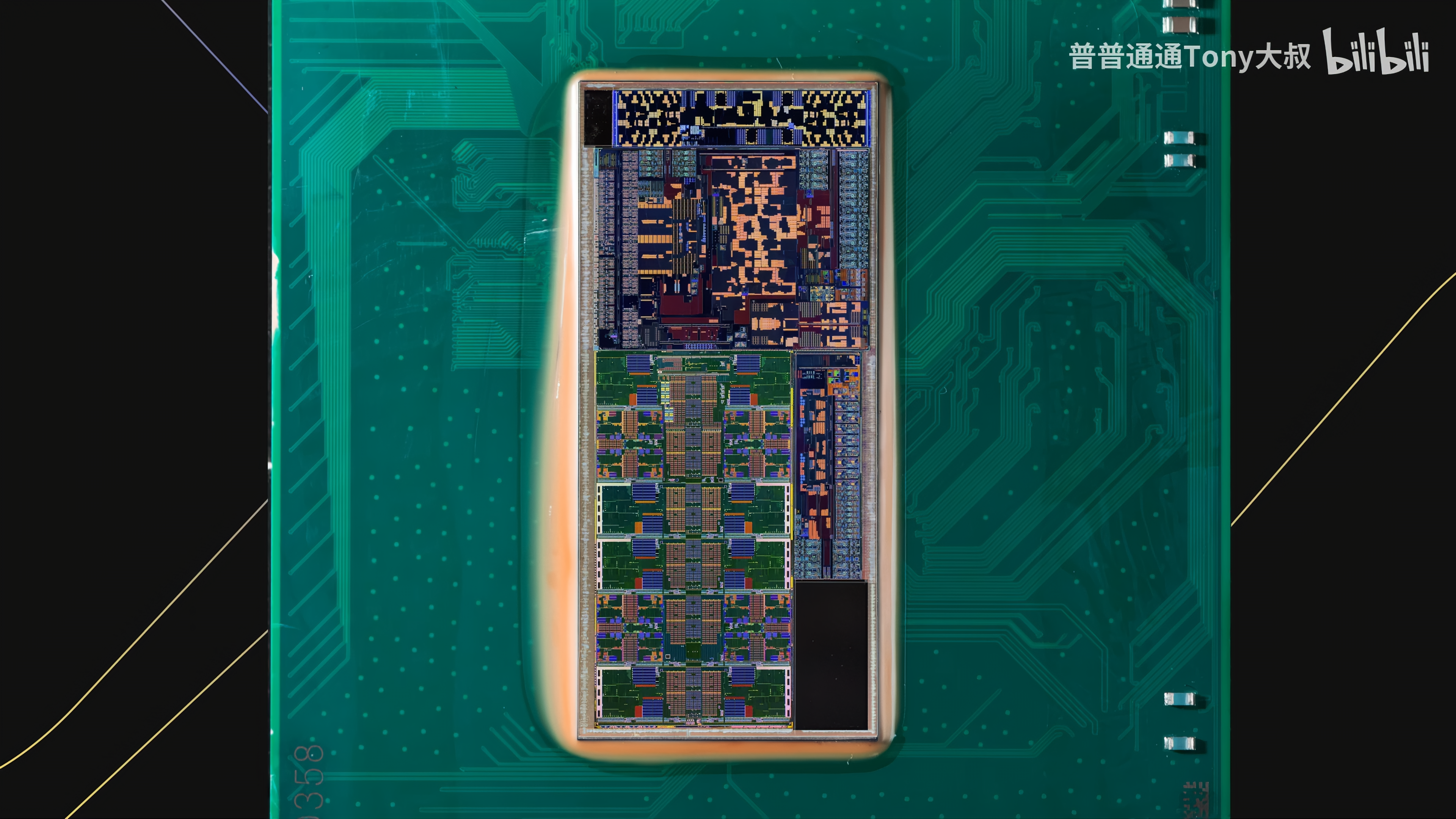
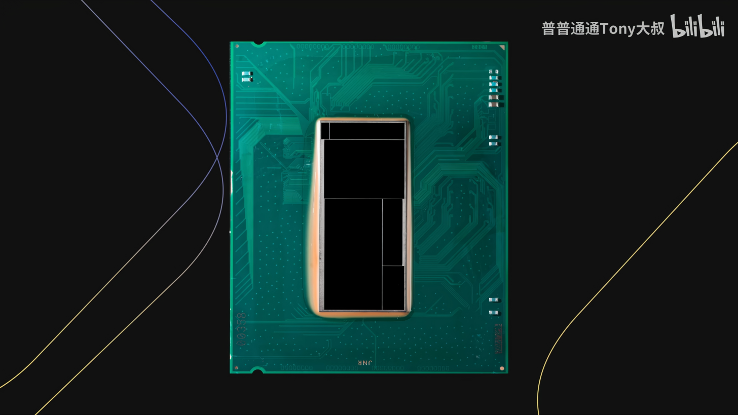
The first official die shots of Intel's Arrow Lake-based Core Ultra 9 285K have surfaced, thanks to Tony Yu at Bilibili, Asus' manager in China. The images delve into Arrow Lake's tile or chiplet architecture, structured using Intel's advanced 3D Foveros packaging technology. We also get a clearer picture of each tile's specific layout and functionality thanks to these close-ups.
Arrow Lake features a total of six tiles; the Compute Tile, the SoC Tile, the IOE Tile, the Graphics Tile, and two Filler Tiles for structural integrity. Underneath these tiles is the active interposer, which categorizes this packaging as a 3D design. Funnily enough, Intel has opted to use TSMC for every tile apart from the Base Tile - which itself is built using an outdated 22nm process node.
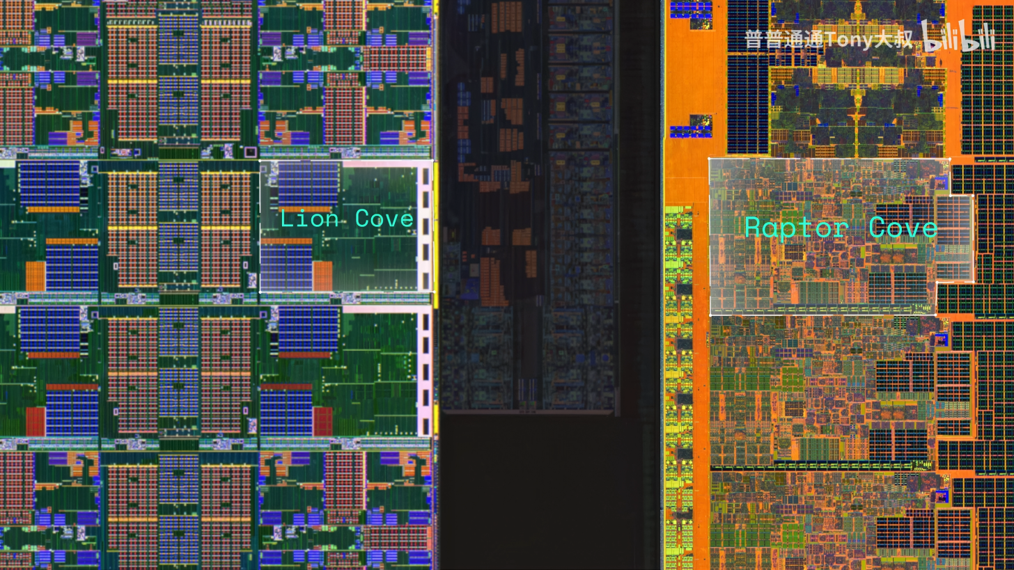
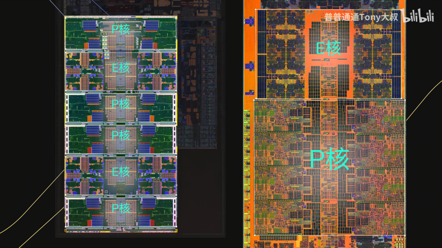
The bulk of the die space is occupied by the Compute Tile which hosts all the cores and cache. A comparison against Raptor Cove-based performance cores used in Intel's 13th Generation shows that Lion Cove is considerably smaller than its predecessor. This can be attributed to the node shrink from Intel 7 to TSMC N3B. Even the core layout is different, as Arrow Lake has the performance cores contiguous with the efficient cores, while in Raptor Lake they were placed at different areas of the die.
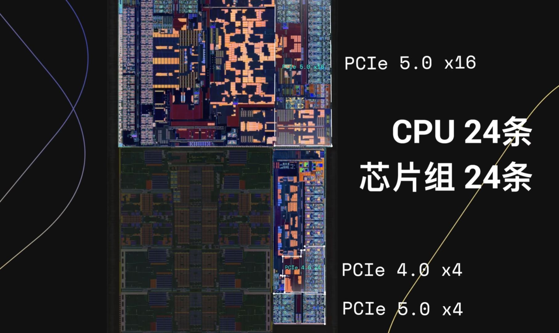
With Arrow Lake, the memory fabric and controllers have been shifted off-die to the SoC Tile - built using TSMC's N6 node. This will introduce latency penalties which, when paired with the already slow ring bus, perhaps explain Arrow Lake's poor gaming performance. The PCIe 5.0 x16 interface for the GPU is situated in the SoC Tile, though interestingly the PCIe 4.0 and 5.0 x4 interconnects for NVMe SSDs have been designated to the IOE Tile.
Furthermore, the SoC Tile also packs Arrow Lake's NPU - said to offer 13 TOPS of AI performance in tandem with the display and media complexes. Being at the center of the package, the SoC Tile will have the most Die to Die interconnects, as it has to communicate with all the chiplets. Since Intel has not explicitly detailed its core-to-uncore connection methodology, it may be safe to assume that data is still routed via the good-old ring bus.
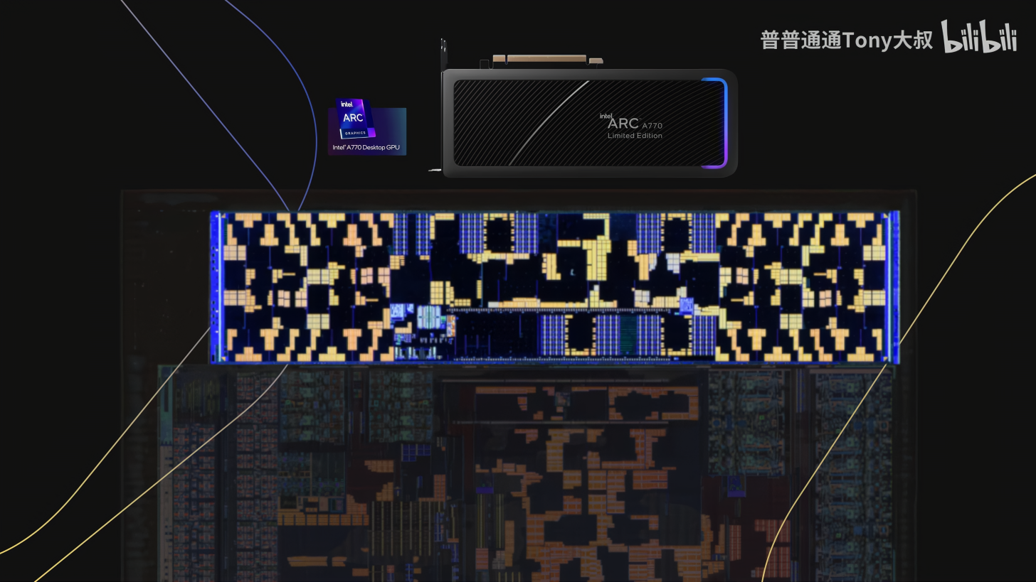
Lastly, four Xe cores based on the Alchemist architecture have been allotted to the GPU Tile - manufactured using TSMC's N5 node. This is the same Xe-LPG architecture seen in Meteor Lake and is inferior to Xe2 (Battlemage) on Lunar Lake and Xe-LPG+ (Alchemist+) expected with Arrow Lake mobile.
This disaggregated approach opens room for insane levels of modularity as Intel can swap any of these tiles according to their preferences. But, as is everything with chiplets or tiles, there is an obvious increase in latency and packaging overhead.
Get Tom's Hardware's best news and in-depth reviews, straight to your inbox.
The Core Ultra 200S series of CPUs will hit shelves the day after tomorrow. Let's hope Arrow Lake is as good as leaks suggest. Stay tuned to Tom's Hardware for detailed reviews sharing the real-world performance of these processors.

Hassam Nasir is a die-hard hardware enthusiast with years of experience as a tech editor and writer, focusing on detailed CPU comparisons and general hardware news. When he’s not working, you’ll find him bending tubes for his ever-evolving custom water-loop gaming rig or benchmarking the latest CPUs and GPUs just for fun.
-
usertests Gorgeous shot, interesting reuse of Meteor Lake. I assume the NPU is copy-pasted from Meteor Lake (with higher clock speed) even if the tile it's on isn't.Reply
Arrow Lake is now Meatier Lake. -
User of Computers Reply
it's rumored that this SoC tile is re-used from the cancelled Meteor Lake-S design. In fact, all tiles except for the compute tiles are allegedly reused from Meteor Lake-S.usertests said:Gorgeous shot, interesting reuse of Meteor Lake. I assume the NPU is copy-pasted from Meteor Lake (with higher clock speed) even if the tile it's on isn't.
Arrow Lake is now Meatier Lake. -
Mama Changa Reply
So? If they had nothing to change, why change it? Compute tile is what's most important, not crappy iGPU or NPU. Panther Lake will fix that aspect if it comes to desktop, which is now rumoured as Arrow Lake refresh is cancelled. Otherwise, I guess we wait for Nova Lake.User of Computers said:it's rumored that this SoC tile is re-used from the cancelled Meteor Lake-S design. In fact, all tiles except for the compute tiles are allegedly reused from Meteor Lake-S.
Any way details are alwasy interesting but I'm waiting for the real benchmarks about performance and efficiency. All leaks are promising on the latter with 285 non K at 65W beating 14900K at 125W. -
usertests Reply
I'm not complaining. There is already disappointment about Arrow Lake not dominating vs. 7800X3D/9950X, but the strengths of tiles/chiplets are starting to show.Mama Changa said:So? If they had nothing to change, why change it? Compute tile is what's most important, not crappy iGPU or NPU. Panther Lake will fix that aspect if it comes to desktop, which is now rumoured as Arrow Lake refresh is cancelled. Otherwise, I guess we wait for Nova Lake.
Any way details are alwasy interesting but I'm waiting for the real benchmarks about performance and efficiency. All leaks are promising on the latter with 285 non K at 65W beating 14900K at 125W.
And I actually like that the "crappy iGPU" is going to be maybe up to twice as fast as the one in Alder/Raptor Lake and Zen 4/5. There will be some nice office PCs on the market with this in it. -
bit_user Reply
Meteor Lake performed poorly, which is partly blamed on its new interconnect topology. Intel ditched it in Lunar Lake and went another direction.Mama Changa said:So? If they had nothing to change, why change it?
It's also believed to be one of the reasons Arrow Lake is delivering such uneven improvements over Raptor Lake. -
bit_user Reply
Since Sandybridge, Intel's iGPUs were always good enough for office PCs. I used an i7-2600K for about a decade, with only integrated graphics. Even at 1440p, it was completely fine.usertests said:And I actually like that the "crappy iGPU" is going to be maybe up to twice as fast as the one in Alder/Raptor Lake and Zen 4/5. There will be some nice office PCs on the market with this in it. -
jp7189 Assuming the core to core latency isn't too bad, I really like the idea of spreading out the hottest spots. That should solve a lot of the thermal throttling situations. Although it also would seem to indicate all P core to core may be going through the soc chiplet which could really tank some workloads.Reply -
bit_user WCCFTech included one that did a size matchup vs. Apple's A17 Pro:Reply
Source: https://wccftech.com/intel-core-ultra-9-285k-cpu-detailed-die-shots-3nm-arrow-lake-compared-10nm-raptor-lake/
However, I think that might be made on TSMC N3E, which makes the comparison off by a few %. -
bit_user Reply
I wonder which are the hot spots, though. In Alder/Raptor Lake, the E-cores had higher thermal density.jp7189 said:Assuming the core to core latency isn't too bad, I really like the idea of spreading out the hottest spots.
I agree that it will be interesting to see core-to-core latency plots, as well as more detailed information about the topology. I wonder if the E-core clusters now have their own L3 slices. -
usertests Reply
True, but when they double the iGPU's gaming performance, it might be enough to take Skyrim 720p to 1080p for example, and improve other games and emulators that are on the brink of being playable. It's nice to have. Ryzen 7000/9000 desktop CPUs have a slower iGPU than this one.bit_user said:Since Sandybridge, Intel's iGPUs were always good enough for office PCs. I used an i7-2600K for about a decade, with only integrated graphics. Even at 1440p, it was completely fine.
Arrow Lake will go into millions of Dell/Lenovo/HP office PCs, and I'll pick it up when they are being "thrown away". Although now we have MLID claiming a new round of instability issues. We should find out if he's crying wolf tomorrow when the review embargo ends.
V_UHVWcfeTg
