Intel details new advanced packaging breakthroughs — EMIB-T paves the way for HBM4 and increased UCIe bandwidth
EMIB-T comes to fore.
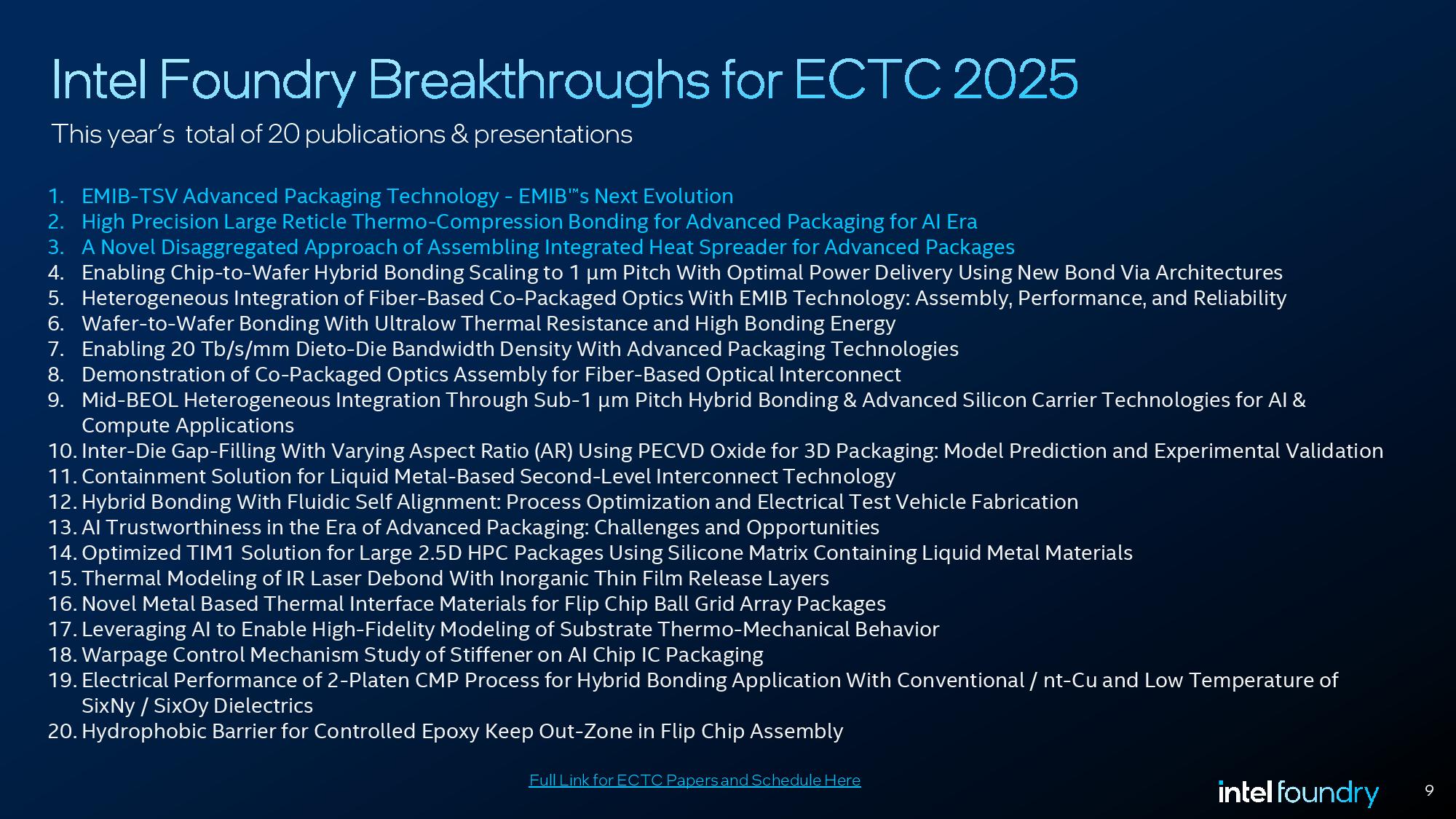
Intel disclosed several chip packaging breakthroughs at the Electronic Components Technology Conference (ECTC), outlining the technical merits of multiple new chip packaging techniques. We spoke with Dr. Rahul Manepalli, an Intel Fellow and VP of Substrate Packaging Development, for more details on three of the new packaging technologies: EMIB-T for boosting both the size of chip packages and power delivery capabilities to support new technologies like HBM4/4e, a new disagregated heat spreader design, and a new thermal bonding technique that improves reliability, yields, and enables scaling to finer chip-to-chip connections. Intel also participated in 17 other new papers presented at the event.
Intel Foundry aims to produce chips for both Intel's own internal use and for external companies, utilizing leading-edge process node technology. However, modern processors are increasingly deployed with complex, heterogeneous designs that integrate multiple types of computing and memory components into a single chip package, thereby amplifying performance, cost, and power efficiency gains. These chip designs rely upon increasingly complex advanced packaging techniques that serve as the bedrock of heterogeneous designs, so continued evolution is critical as Intel keeps pace with competitors like TSMC.
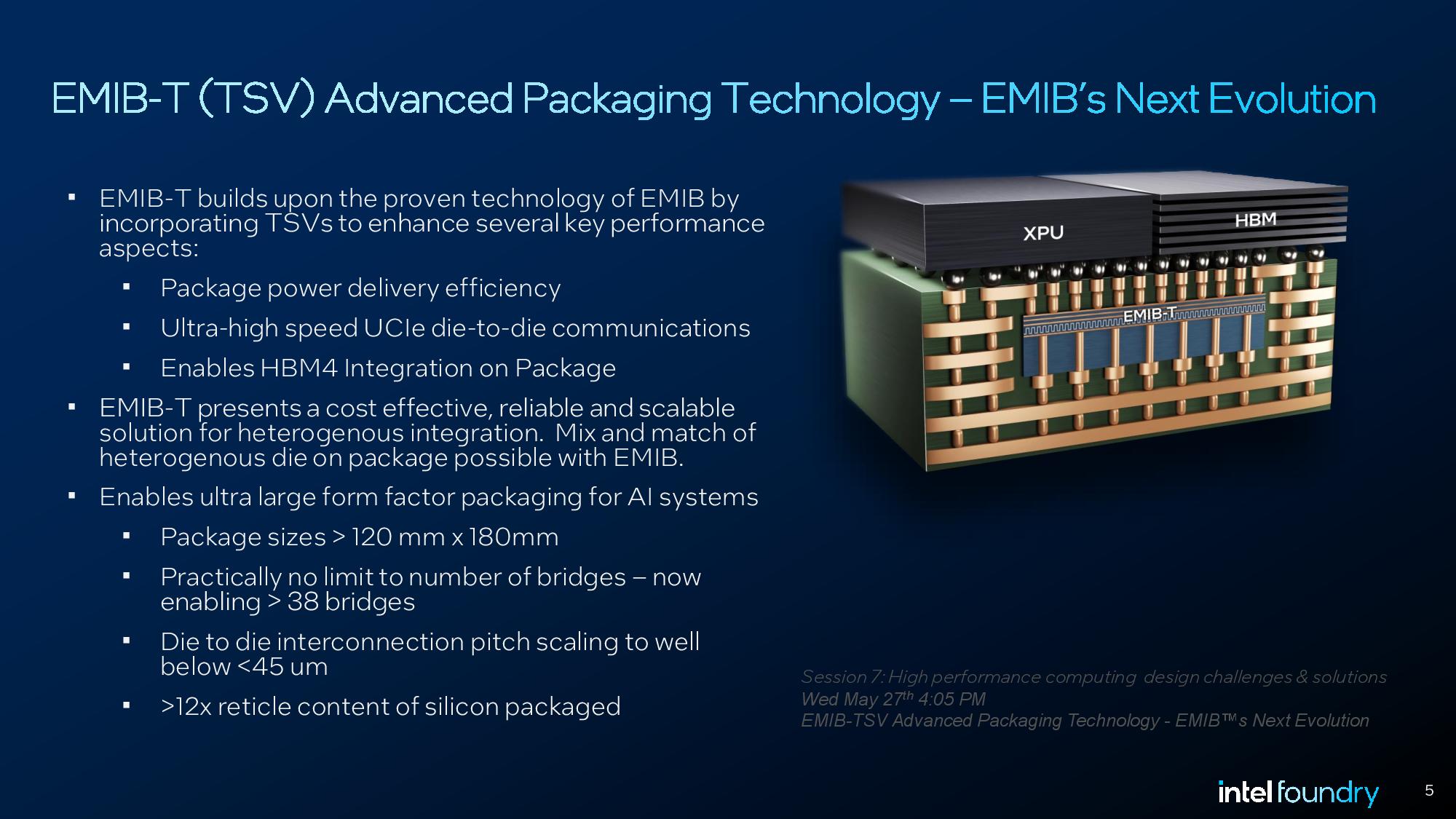

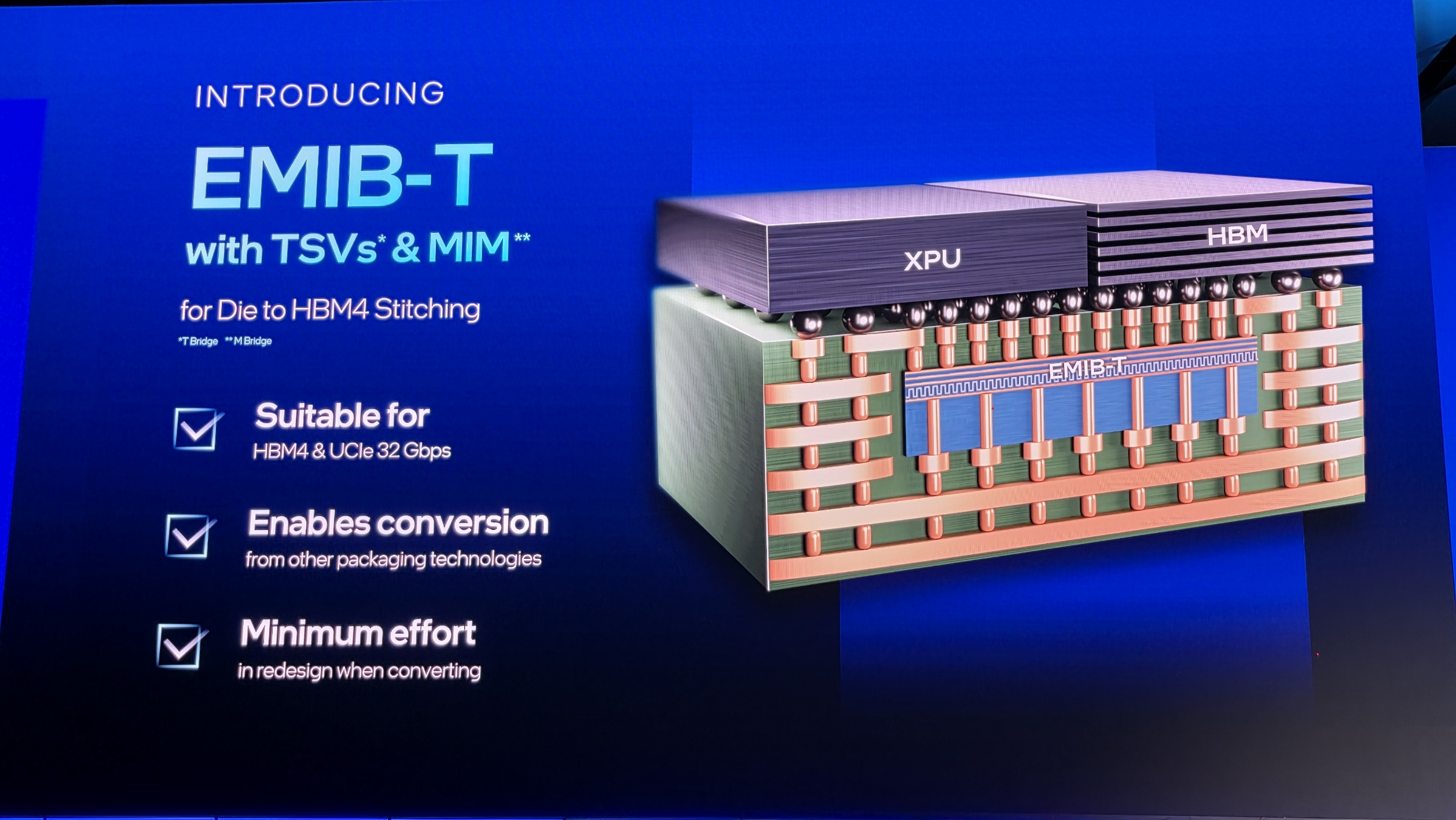
Intel's new EMIB-T, originally disclosed at its Intel Direct Connect event last month, incorporates through-silicon vias (TSVs) into its already widely used EMIB technology —a silicon bridge embedded in a package substrate that provides communication and power plumbing between chiplets/dies.
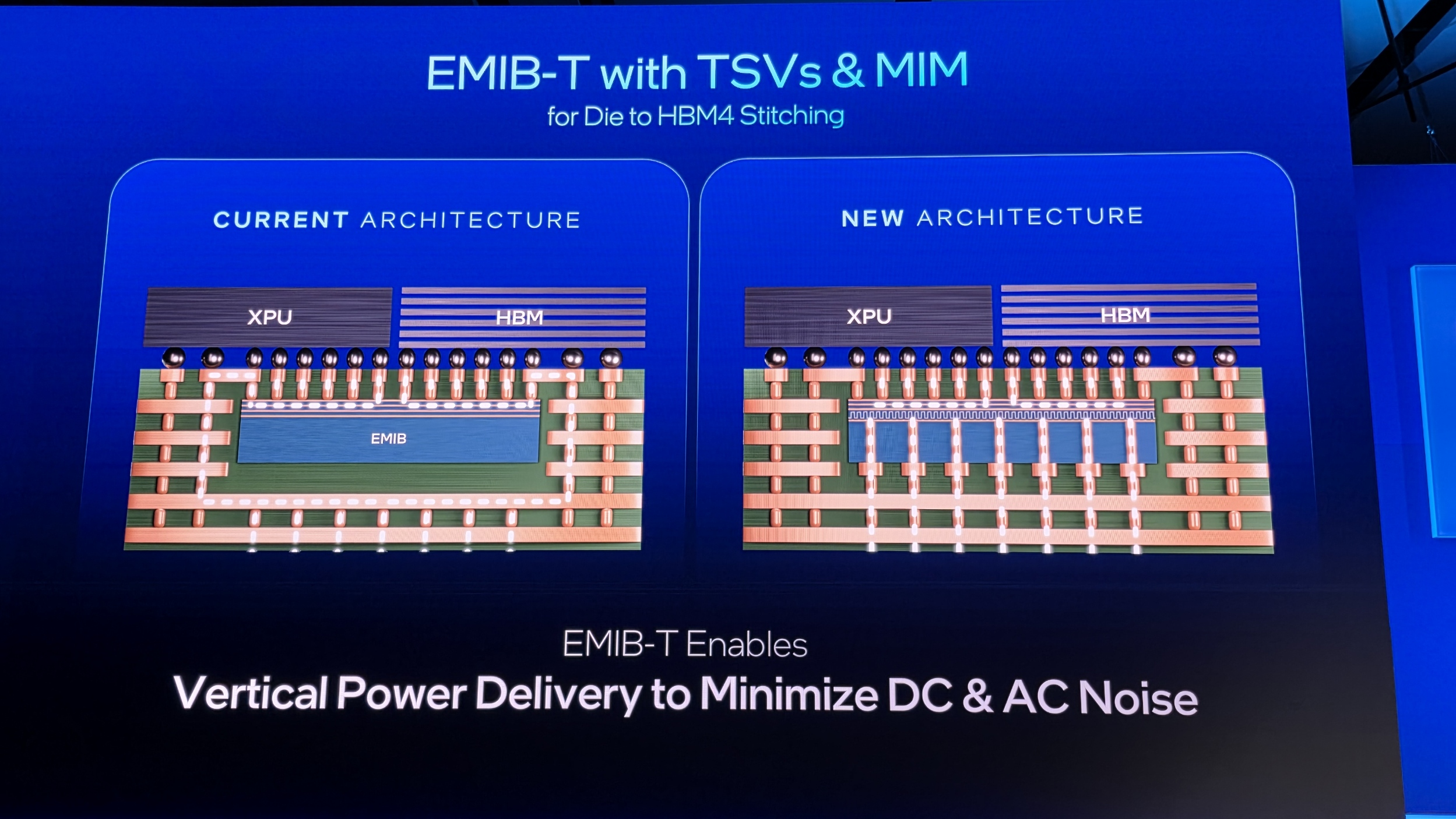
This next evolution of EMIB enhances critical package power delivery efficiency metrics and speeds die-to-die communication. EMIB-T can be used to more effectively power compute and memory components — whereas standard EMIB connections struggled with high voltage droop due to a cantilevered power delivery path, EMIB-T utilizes TSVs to provide power delivery from the bottom of the chip package via TSV bridge dies, thus enabling a direct, low-resistance path for power delivery that's critical for HBM4/4e integration.
Naturally, the use of TSVs also boosts die-to-die communication bandwidth, enabling the integration of high-speed HBM4/4e memory packages and the use of the UCIe-A interconnect to increase data transfer rates to 32 Gb/s or higher. Routing power and signals through the same interface introduces 'noise' in the signal path, but Intel integrated high-powered MIM capacitors into the bridge to help ensure consistent communication signaling.
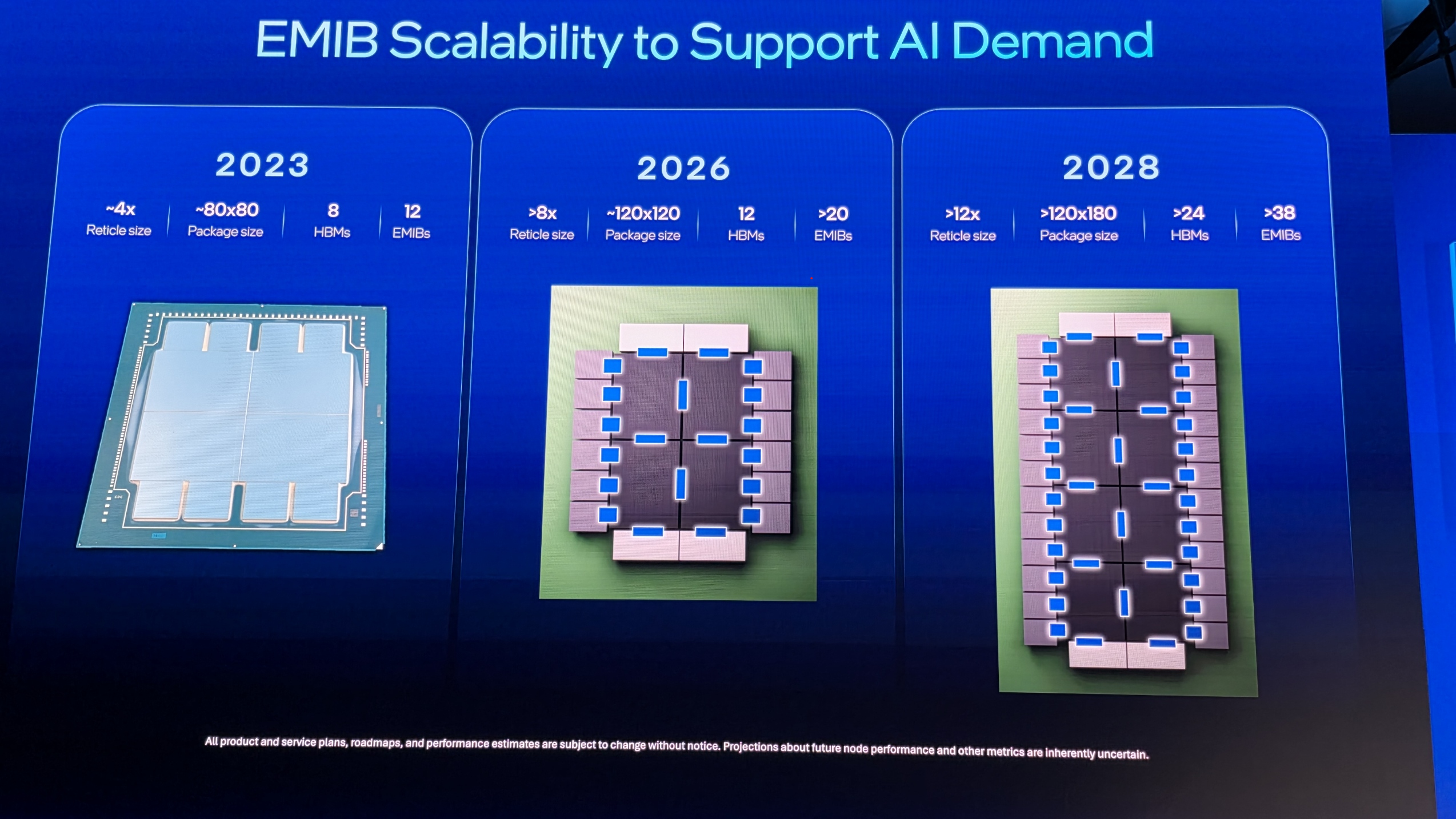
EMIB-T also enables much larger chip package sizes, reaching 120x180mm, and supports more than 38 bridges and more than 12 recticle-sized die in a single large chip package. Additionally, the first generation of EMIB enabled a 55-micron bump pitch, a critical interconnect density metric, while the second-generation EMIB scaled down to a 45-micron pitch. Intel's paper demonstrates an EMIB-T design with a 45-micron pitch, but notes that the new technology supports "well below" 45-micron pitches, saying it will go to 35-micron pitches soon and has 25-micron pitches in development. Intel hasn't shared the picojoules-per-bit (pJ/bit) power efficiency metrics. EMIB-T is also compatible with either organic or glass substrates, with the latter being a key strategic direction for Intel's future chip packaging endeavors.
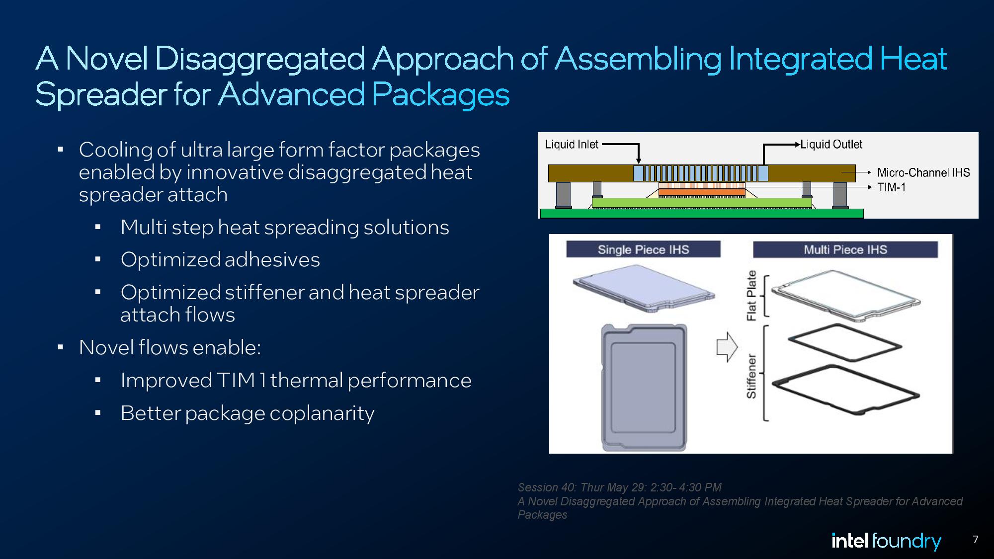
The AI revolution is pushing chip package sizes to new frontiers, and with that comes increased power consumption that introduces vexing cooling challenges. Intel also disclosed a new disaggregated heat spreader technique that breaks the heat spreader into a flat plate and a stiffener to improve coupling between the heat spreader and the thermal interface material (TIM) that resides between the heat spreader and the underlying die. Among other benefits, this technique helps reduce voids in solder TIM coupling by 25%.
Get Tom's Hardware's best news and in-depth reviews, straight to your inbox.
Intel's illustration shows a heatspreader with integrated micro-channels that carry liquid directly through the IHS to cool the processor, much like we saw on display at its Direct Connect event. While the paper focused on the effects of breaking the heatspreader into multiple pieces, the inclusion of this tech, which can cool processor packages with a TDP up to 1000W, highlights that Intel is approaching the chip cooling problem from multiple angles.
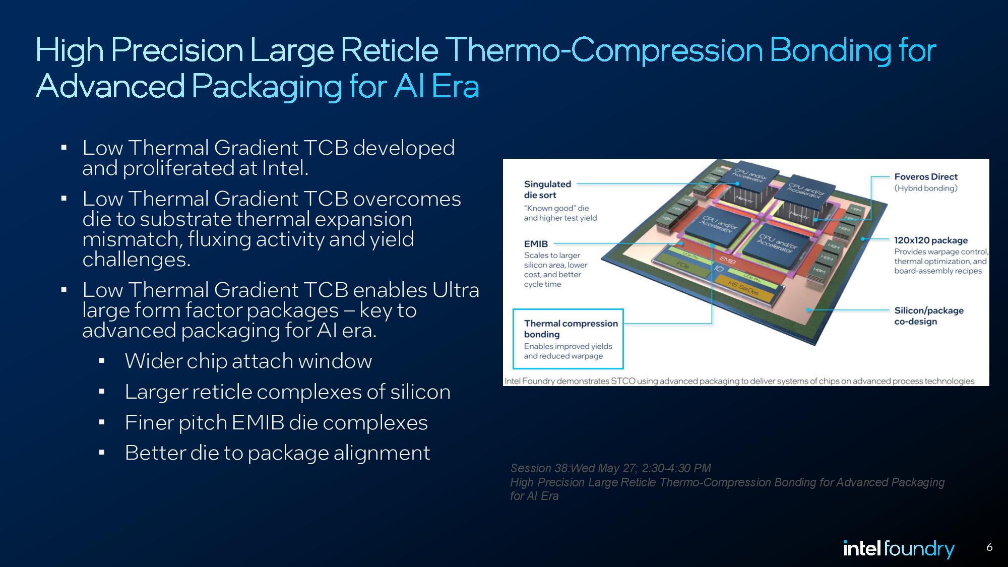
Intel has utilized thermal compression bonding techniques in both its server and consumer products; however, it has now developed a new thermal compression bonding process specifically for large package substrates that helps overcome die and substrate warpage during the bonding process.
This new technique minimizes the thermal delta between the package substrate and the die during the bonding process, thereby improving yield and reliability metrics and enabling much larger chip packages than are currently possible in high volume manufacturing. It also enables finer pitches for EMIB connections, helping to squeeze out more density from EMIB-T technology.
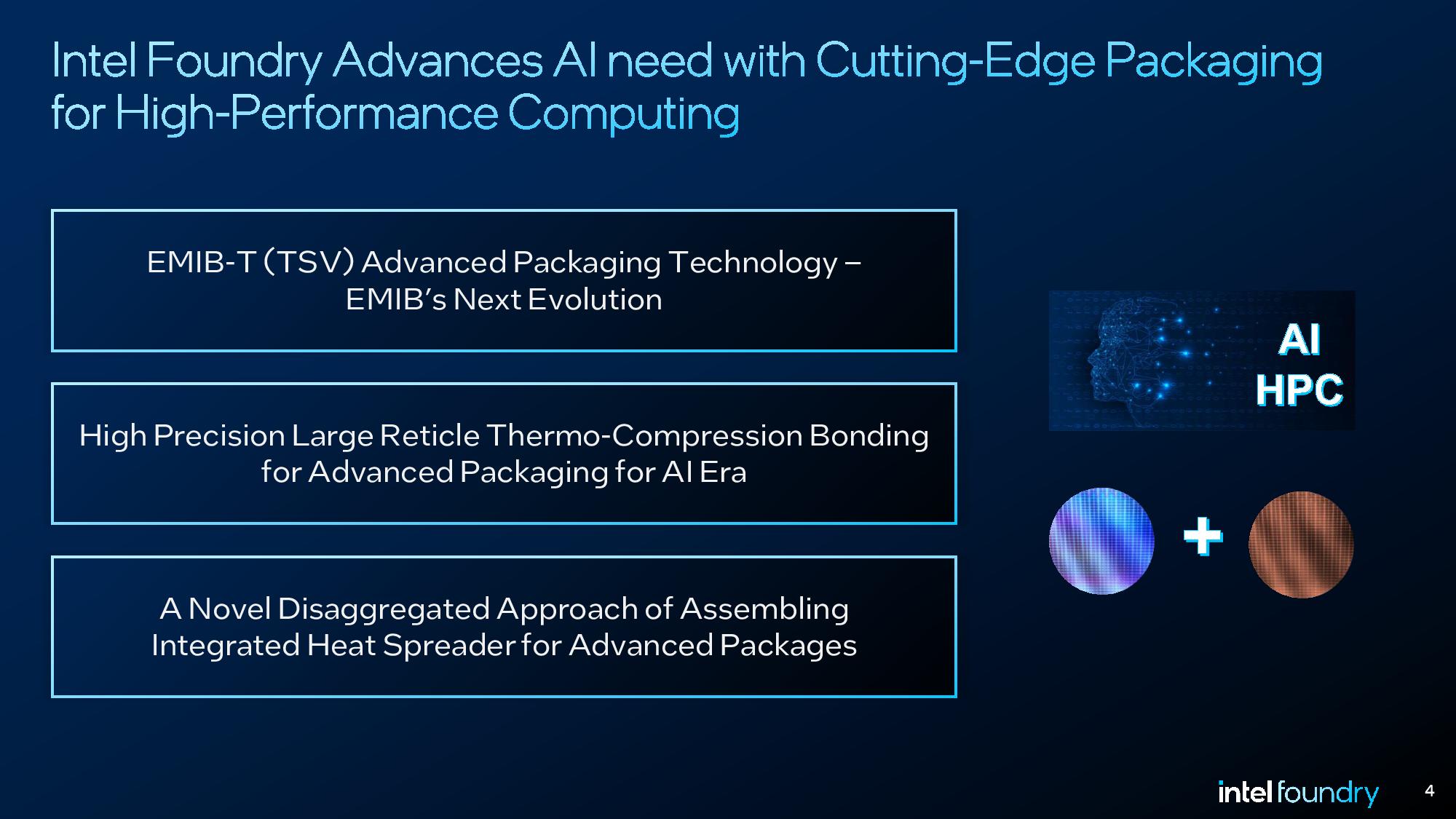
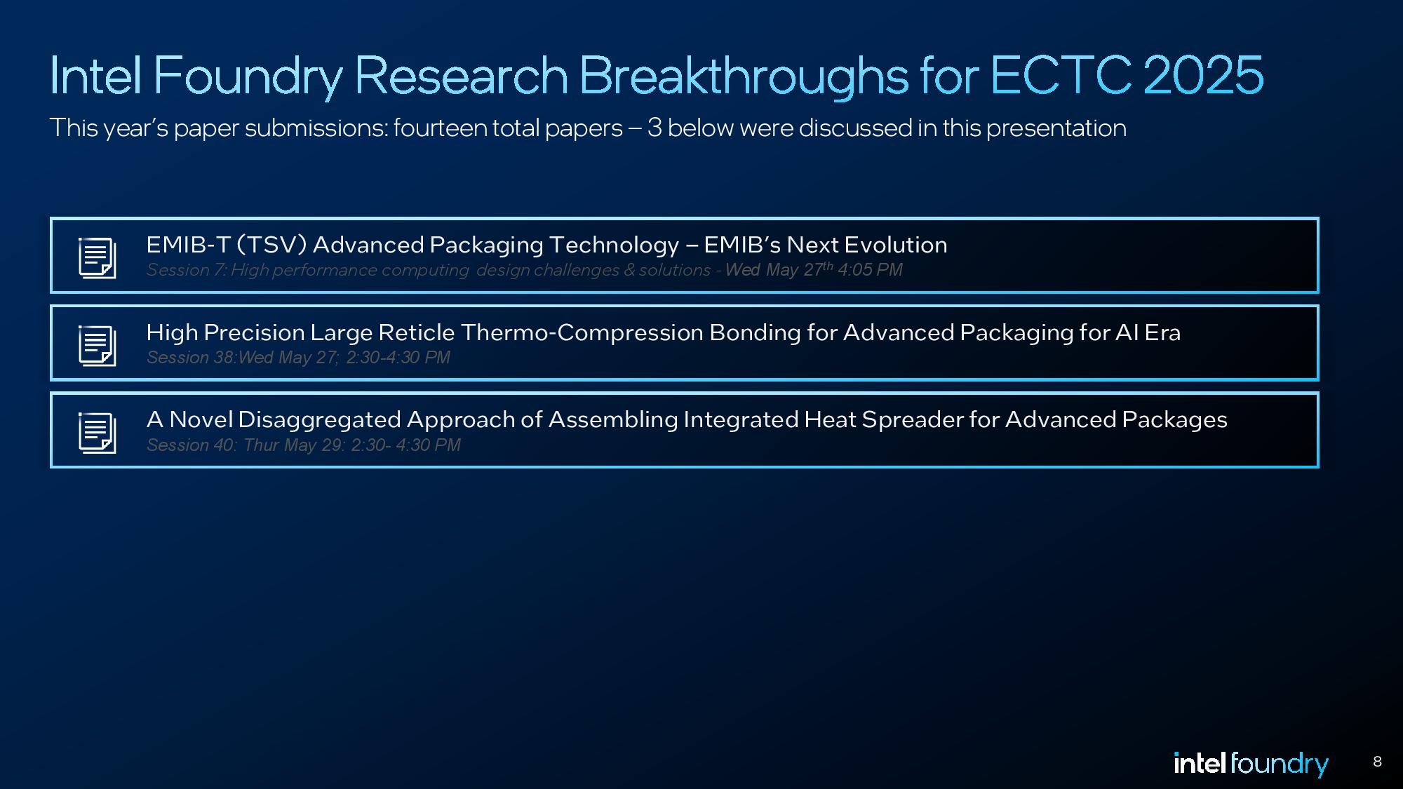

Having a well-rounded and competitive suite of packaging technologies is crucial for Intel Foundry as it aims to provide its customers with the most comprehensive range of chip production options possible. Advanced chip packaging techniques enable customers to integrate different types of chips, such as CPUs, GPUs, and memory, from multiple vendors into a single package, thereby reducing the risk of transitioning entirely to Intel's process nodes for all componentry. In fact, Intel also offers packaging services for chips that don't use any Intel-fabbed components at all, helping to build relationships with potential new customers for its chip-fabbing services.
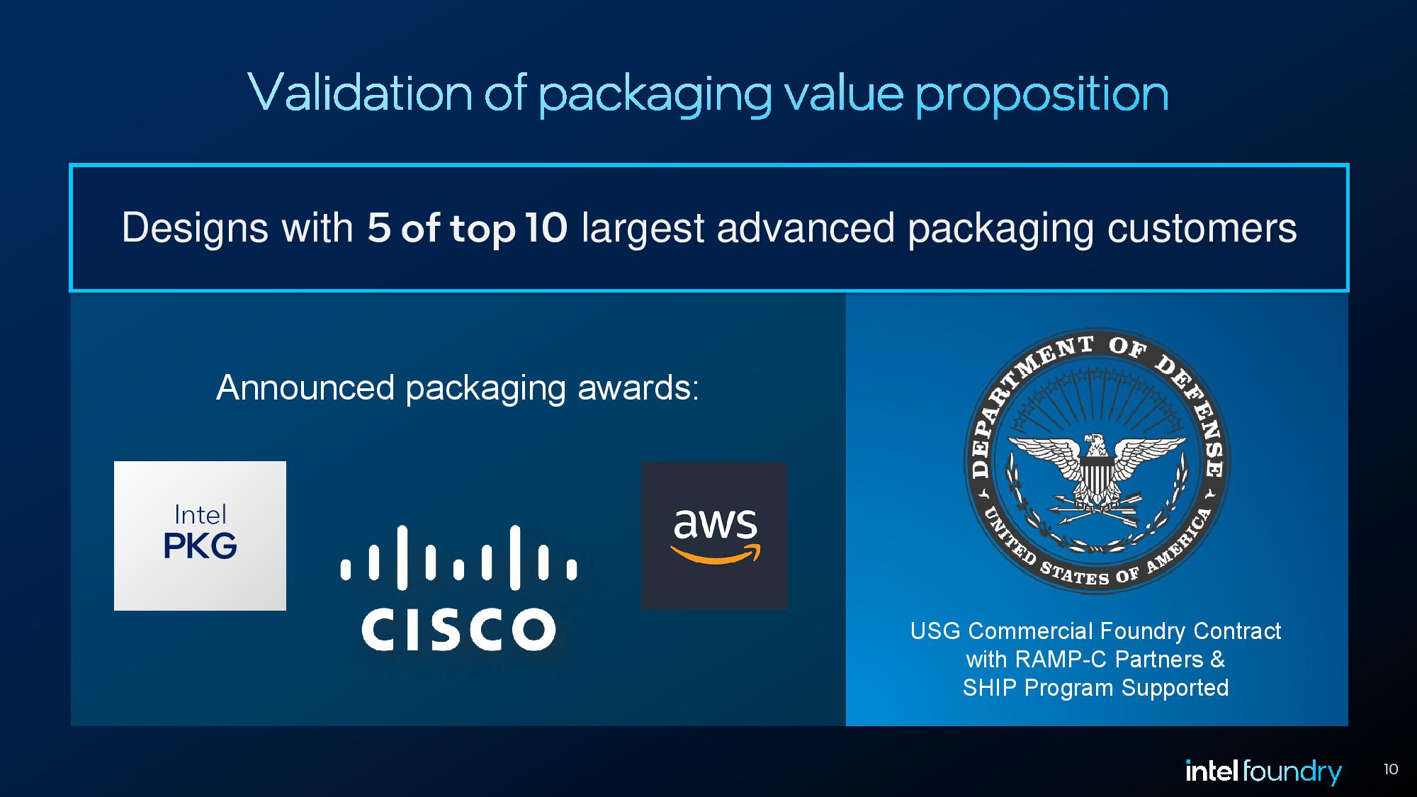
Chip packaging has also emerged as one of the leading services for Intel's external customers, which currently include industry heavyweights such as AWS and Cisco, among others, as well as the US government's RAMP-C and SHIP projects. These packaging contracts serve as the fastest on-ramp for Intel Foundry revenue generation, as producing chips with leading-edge process nodes requires significantly longer lead times.

Paul Alcorn is the Editor-in-Chief for Tom's Hardware US. He also writes news and reviews on CPUs, storage, and enterprise hardware.
-
thestryker It's really interesting to see the innovations being made for the huge sizes enterprise level chips have gotten to. Hopefully some of the connectivity advances will make its way down toReply
For whatever reason when I'd read about EMIB-T before my brain just didn't put two and two together that the TSVs were through the EMIB silicon itself. I thought it was supposed to make its debut with CWF, but that doesn't seem to be the case. It'll be interesting to see if maybe there will be a DMR "Max" like we saw with SPR. -
Pierce2623 I hope they end up with actual volume capabilities in the 2.5d stuff. I feel like Arrow Lake/Lunar Lake already approached the maximum bandwidth available on their currently used interposer technology. Core to core latency through the interposer was terrible for cores on a seperate die on Lunar Lake and LL is generally much better on latency than Arrow Lake.Reply -
thestryker Reply
LNL/ARL didn't use EMIB and the chances of anything client using it are pretty low. Everything was placed on a base tile utilizing Foveros, and there are several different versions of that. It's more likely latency is a design level issue rather than interconnect because Intel's physical interconnect is superior to AMD's.Pierce2623 said:I hope they end up with actual volume capabilities in the 2.5d stuff. I feel like Arrow Lake/Lunar Lake already approached the maximum bandwidth available on their currently used interposer technology. Core to core latency through the interposer was terrible for cores on a seperate die on Lunar Lake and LL is generally much better on latency than Arrow Lake. -
acadia11 So the more I think about it, Intel should really spin off foundry unit as a subsidiary or separate company. No partner is really going to trust Intel if they are also competing with Intel for resources as a contract client. Samsung and TSMC are its main competitors on the foundry side but you notice TSMC doesn’t compete with its clients but serves them. And this is one of the reasons they are massively successful. Samsung does but it has proven track record as a sourcing partner.Reply -
TerryLaze Reply
What exactly is the trust that partners are going to have???acadia11 said:So the more I think about it, Intel should really spin off foundry unit as a subsidiary or separate company. No partner is really going to trust Intel if they are also competing with Intel for resources as a contract client. Samsung and TSMC are its main competitors on the foundry side but you notice TSMC doesn’t compete with its clients but serves them. And this is one of the reasons they are massively successful. Samsung does but it has proven track record as a sourcing partner.
Everybody is going to keep using tsmc and then intel additionally to that so they won't have to worry about losing out on selling stuff.
And if intel doesn't provide them the amount of product they agreed upon they will be able to sue intel because everything is done with contracts.
Intel isn't some shady 3rd country business nobody has heard about before, they have 50+ years of business relations to everybody in the business. -
thestryker Reply
This isn't a viable business plan until the vast majority of Intel's silicon production uses industry standard tools. Perhaps 2027-2028 at the very earliest, but I wouldn't be surprised if the future was already locked in by then.acadia11 said:So the more I think about it, Intel should really spin off foundry unit as a subsidiary or separate company. No partner is really going to trust Intel if they are also competing with Intel for resources as a contract client. Samsung and TSMC are its main competitors on the foundry side but you notice TSMC doesn’t compete with its clients but serves them. And this is one of the reasons they are massively successful. Samsung does but it has proven track record as a sourcing partner. -
acadia11 Reply
18A is “supposedly” following industry standard specifications , but yes 14A is supposedly when Intel feels it will have made the full transition as a partner foundry.thestryker said:This isn't a viable business plan until the vast majority of Intel's silicon production uses industry standard tools. Perhaps 2027-2028 at the very earliest, but I wouldn't be surprised if the future was already locked in by then. -
thestryker Reply
EUV isn't the problem, as all of their EUV nodes are standardized, it's the DUV nodes that are the problem. They have a massive amount of DUV capacity and outside of Intel 16 (a modified 22nm) none of them adhere to standards. There's also a forthcoming 'Intel 12' node they're developing with UMC which has been forecast for ~2027. They have to be able to covert a majority of their DUV capacity before the foundry business could be viable on its own.acadia11 said:18A is “supposedly” following industry standard specifications , but yes 14A is supposedly when Intel feels it will have made the full transition as a partner foundry. -
Pierce2623 Reply
I’m aware they didn’t use EMIB. That’s my point. Their current client interposer solution sucks.thestryker said:LNL/ARL didn't use EMIB and the chances of anything client using it are pretty low. Everything was placed on a base tile utilizing Foveros, and there are several different versions of that. It's more likely latency is a design level issue rather than interconnect because Intel's physical interconnect is superior to AMD's. -
Pierce2623 Reply
That 12nm could be their golden goose for cheap commercial chip production too.thestryker said:EUV isn't the problem, as all of their EUV nodes are standardized, it's the DUV nodes that are the problem. They have a massive amount of DUV capacity and outside of Intel 16 (a modified 22nm) none of them adhere to standards. There's also a forthcoming 'Intel 12' node they're developing with UMC which has been forecast for ~2027. They have to be able to covert a majority of their DUV capacity before the foundry business could be viable on its own.