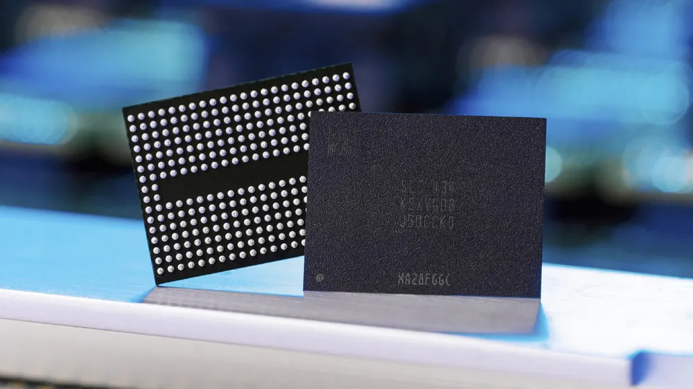
Samsung has introduced its upcoming 10th-generation V-NAND flash memory with over 400 active layers and a 5.6 GT/s interface speed at the International Solid-State Circuit Conference 2025. The new type of memory not only boasts a record number of active layers and groundbreaking performance (which will enable some of the best SSDs), but it also uses Samsung's cell-on-peripheral (CoP) architecture with hybrid bonding, a first for Samsung.
The 10th Gen V-NAND device that Samsung presented at ISSCC is a 3D TLC NAND device with over 400 active layers, a 1 Tb capacity per die, and a 5.6 GT/s interface speed. As the new memory IC continues to use a triple-level cell design, it offers a 28 Gb/mm^2 density, which is slightly lower compared to Samsung's 1Tb 3D QLC V-NAND, which reaches 28.5 Gb/mm^2. However, density may not be Samsung's main goal with this particular product as the key innovations that it introduces are the record number of active layers (over 400) and hybrid bonded periphery circuitry.
| Header Cell - Column 0 | YMTC | YMTC | Micron | Samsung | Samsung | Kioxia/Sandisk | Kioxia/Sandisk | SK hynix |
|---|---|---|---|---|---|---|---|---|
| Generation | ? | Xtacking 3.0/Gen 4 | Gen 9 (G9) | V9 | V10 | BiCS 8 | BiCS 9 | Gen 9 |
| Layers | 232-Layer | 232-Layer | 276-Layer | 290-Layer (?) | 4xx-Layer | 218-Layer | 332-Layer | 321-Layer |
| Density | >20 Gb mm^2 | 19.8 Gb mm^2 | 21.0 Gb mm^2 | 17 Gb mm^2 | 28 Gb mm^2 | 22.9 Gb mm^2 (?) | ? | 20 mm^2 |
| Architecture | TLC | QLC | TLC | TLC | TLC | QLC | ? | TLC |
| Die Capacity | 1 Tb | 1 Tb | 1 Tb | 1 Tb | 1 Tb | 2 Tb | ? | 1 Tb |
| I/O Speed | ? | ? | Up to 3600 MT/s | Up to 3200 MT/s | Up to 5600 MT/s | Up to 3600 MT/s | Up to 4800 MT/s | ? |
While Samsung, just like other makers of NAND, has placed peripheral circuitry below the memory array for some time now, with its 10th Generation V-NAND, the company produces peripheral circuits (featuring row decoders, sense amplifiers, buffers, voltage generators, I/O) on a separate wafer using its logic technology. Then, it bonds it to the wafer with a 3D NAND memory array. Other leading makers of 3D NAND memory — including Kioxia/Sandisk and YMTC — also produce 3D NAND array and periphery on different wafers and then bond them together.
Such an architecture enabled Samsung to dramatically increase the interface speed of its 10th Gen V-NAND memory to 5.6 GT/s. At this rate, a single NAND device can offer a peak transfer rate of 700 MB/s. In larger configurations, ten of these could fully utilize a PCIe 4.0 x4 interface, while twenty would max out a PCIe 5.0 x4 connection. A setup with 32 dies across two NAND packages would push performance close to the limits of PCIe 6.0 x4.
Most NAND packages on SSDs are built with either eight or 16 dies. A package containing sixteen dies can store up to 2TB, meaning that four in a single-sided SSD would provide 8TB of capacity. A dual-sided M.2 2280 drive could double that to 16 terabytes. However, Samsung has not released a new dual-sided SSD in recent years as they are not compatible with the vast majority of notebooks.
Without any doubt, Samsung's 10th Generation V-NAND's increased bandwidth and capacity could play a crucial role in next-generation storage devices as these devices enable Samsung to build ultra-high-performance SSDs and UFS modules with competitive capacity points. However, market availability of such products will depend on how quickly Samsung ramps up its latest 3D TLC V-NAND. Yet, Samsung has not yet disclosed when its 10th Gen V-NAND will be incorporated into its own SSD lineup.
