SK hynix announces the world's first 48GB 16-Hi HBM3E memory — Next-gen PCIe 6.0 SSDs and UFS 5.0 storage are also in the works
SK hynix touts a 32% performance increment in inference vs its 12-Hi offerings.

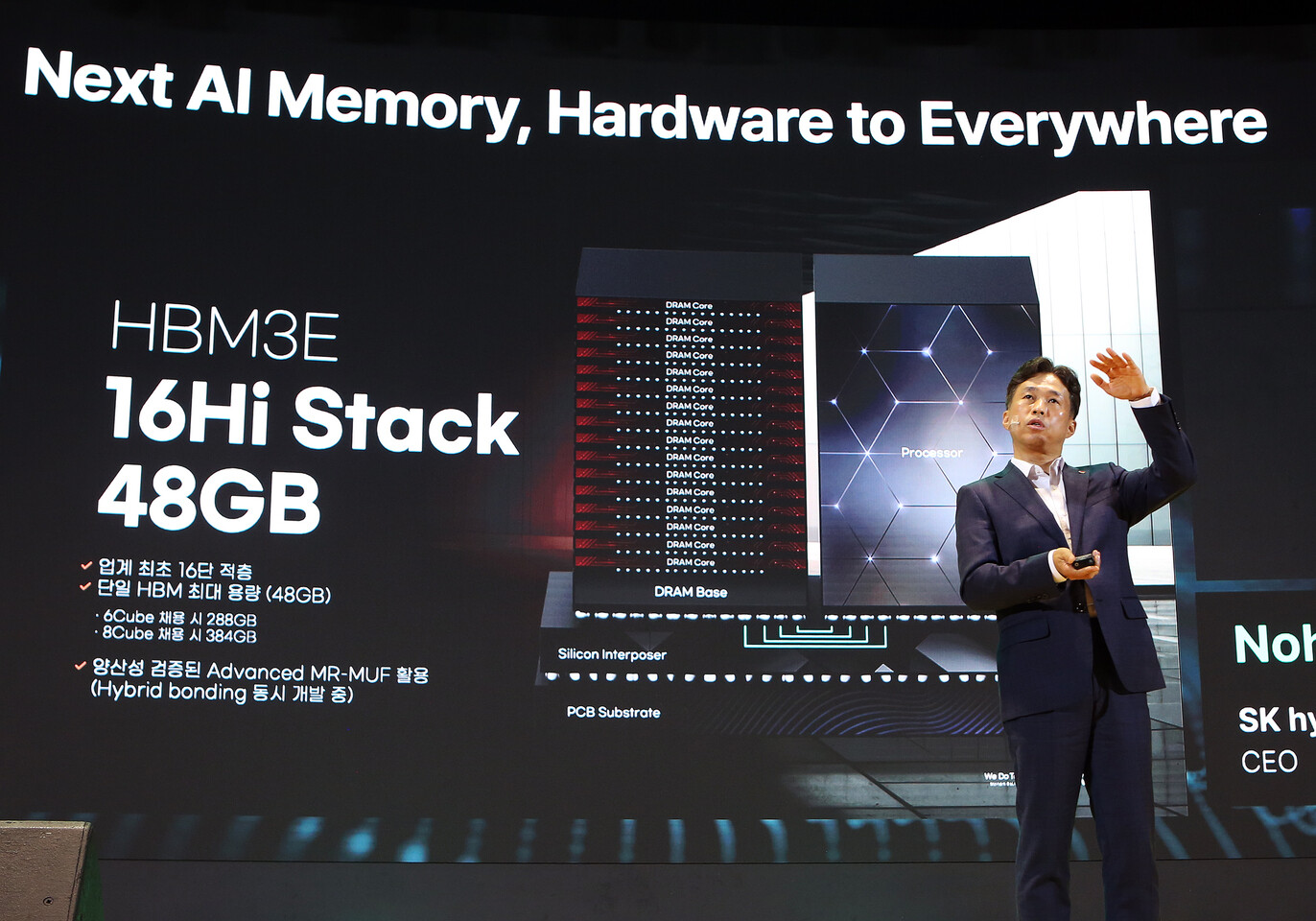
At the SK AI Summit 2024, SK hynix CEO took the stage and revealed the industry's first 16-Hi HBM3E memory - beating both Samsung and Micron to the punch. With the development of HBM4 going strong, SK hynix prepared a 16-layer version of its HBM3E offerings to ensure "technological stability" and aims to offer samples as early as next year.
A few weeks ago, SK hynix unveiled a 12-Hi variant of its HBM3E memory - securing contracts from AMD (MI325X) and Nvidia (Blackwell Ultra). Raking in record profits last quarter, SK hynix is in full steam once again as the giant has just announced a 16-layer upgrade to its HBM3E lineup, boasting capacities of 48GB (3GB per individual die) per stack. This increase in density now allows AI accelerators to feature up to 384GB of HBM3E memory in an 8-stack configuration.
SK hynix claims an 18% improvement in training alongside a 32% boost in inference performance. Like its 12-Hi counterpart, the new 16-Hi HBM3E memory incorporates packaging technologies like MR-MUF which connects chips by melting the solder between them. SK hynix expects 16-Hi HBM3E samples to be ready by early 2025. However, this memory could be shortlived as Nvidia's next-gen Rubin chips are slated for mass production later next year and will be based on HBM4.

That's not all as the company is actively working on PCIe 6.0 SSDs, high-capacity QLC (Quad Level Cell) eSSDs aimed at AI servers, and UFS 5.0 for mobile devices. In addition, to power future laptops and even handhelds, SK hynix is developing an LPCAMM2 module and soldered LPDDR5/6 memory using its 1cnm-node. There isn't any mention of CAMM2 modules for desktops, so PC folk will need to wait - at least until CAMM2 adoption matures.
To overcome what SK hynix calls a "memory wall", the memory maker is developing solutions such as Processing Near Memory (PNM), Processing in Memory (PIM), and Computational Storage. Samsung has already demoed its version of PIM - wherein data is processed within the memory so that data doesn't have to move to an external processor.
HBM4 will double the channel width from 1024 bits to 2048 bits while supporting upwards of 16 vertically stacked DRAM dies (16-Hi) - each packing up to 4GB of memory. Those are some monumental upgrades, generation on generation, and should be ample to fulfill the high memory demands of upcoming AI GPUs.
Samsung's HBM4 tape-out is set to advance later this year. On the flip side, reports suggest that SK hynix already achieved its tape-out phase back in October. Following a traditional silicon development lifecycle, expect Nvidia and AMD to receive qualification samples by Q1/Q2 next year.
Stay On the Cutting Edge: Get the Tom's Hardware Newsletter
Get Tom's Hardware's best news and in-depth reviews, straight to your inbox.
The SK AI Summit 2024 is being held at COEX Convention Center in Seoul November 4-5. The event is the largest AI symposium in Korea, the company claimed.

Hassam Nasir is a die-hard hardware enthusiast with years of experience as a tech editor and writer, focusing on detailed CPU comparisons and general hardware news. When he’s not working, you’ll find him bending tubes for his ever-evolving custom water-loop gaming rig or benchmarking the latest CPUs and GPUs just for fun.
-
newtechldtech I dont understand why Phone makers are insisting on UFS technology while NVME is faster and already here ... Apple has been using NVME in their iPhone for years now.Reply -
pclaughton Reply
Because NVMe consumes more power. If storage speed isn't the bottleneck, why kneecap battery life for shiny specs?newtechldtech said:I dont understand why Phone makers are insisting on UFS technology while NVME is faster and already here ... Apple has been using NVME in their iPhone for years now. -
shawman123 Reply
yah. All phones are fast enough. We obsess over benchmarks. There is nothing we do with it that needs Nvme speeds in a phone. Even UFS is way faster than any workloads on a phone.pclaughton said:Because NVMe consumes more power. If storage speed isn't the bottleneck, why kneecap battery life for shiny specs? -
newtechldtech Reply
Iphones battery life are top charts! and they use NVME technology.pclaughton said:Because NVMe consumes more power. If storage speed isn't the bottleneck, why kneecap battery life for shiny specs?
https://www.gsmarena.com/battery-test-v2.php3 -
pclaughton Reply
Yes, Apple's design let's them get away with using a more power-hungry standard. That hardly means others should switch. Correlation does not imply causation.newtechldtech said:Iphones battery life are top charts! and they use NVME technology.
https://www.gsmarena.com/battery-test-v2.php3 -
newtechldtech Reply
nah , it is just the cost. has nothing to do with power consumption. Even with Tablets with huge batteries , Android Tablet makers are not using NVME ... and at the same time Apple still wins in battery life.pclaughton said:Yes, Apple's design let's them get away with using a more power-hungry standard. That hardly means others should switch. Correlation does not imply causation.
Also , I need Proof that NVME used in Apple iphone uses more power that really matters in battery life ...