Making Motherboards The Gigabyte Way
Get Tom's Hardware's best news and in-depth reviews, straight to your inbox.
You are now subscribed
Your newsletter sign-up was successful
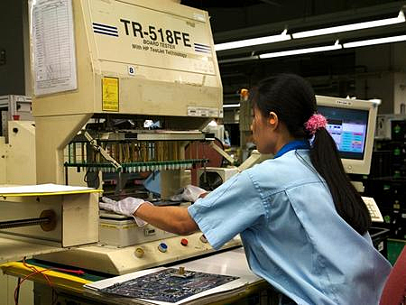
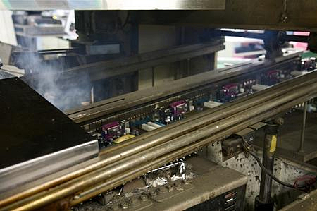
In addition to the visual inspection, the boards are tested electrically, using this machine. Contacts are made at certain predetermined control points. If everything is functioning properly, the PCB is then sent to the manual assembly lines.
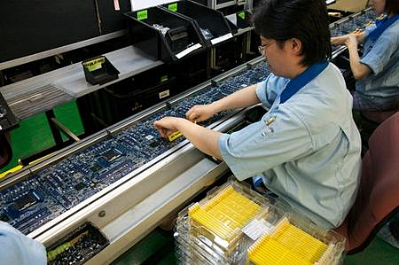
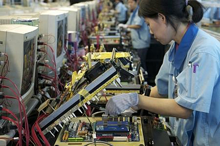
The majority of the components are now soldered to the board, but quite a few still need to be installed. They are referred to as DIPs, for Dual In-line Package, and generally have two rows of pins. These pins are inserted into the corresponding holes on the motherboard and are then soldered on. DIP components are different from SMT ones in that they’re soldered on the opposite side of the PCB. Today, DIPs are used only for components that SMT cannot place or solder. This includes PCI slots, rear connectors, SATA and USB connectors—any component that will undergo strong mechanical stresses.
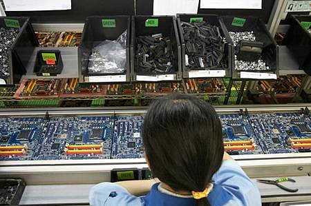
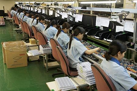
All these components are first placed by hand. The work is done assembly-line style. Each operator adds one component to the PCB, which then moves on to the next worker. Every station has one or more bins of components the worker picks from. The stations at the end of the line are in charge of checking all the components for proper positioning, sometimes by tapping on them, to make sure that all pins are seated in the proper holes.
These manual lines are even more flexible than the SMT machines. As an example, Gigabyte can change the model of the board being produced in 15 minutes on the DIP lines, compared to 30 minutes for SMT.
After the almost fully automated assembly lines, these manned (most are actually populated by women) lines surprised us – especially because of how quiet they are. Except for the clicking of components knocking together, not a whisper breaks the silence. To guarantee a high work cadence, illuminated signboards on each line show the current performance rate in comparison to the objectives for the day.
Once all the components are in place, they have to be soldered to the circuit board. This is no longer done manually. The process is instead completed in a single pass called “wave soldering, ” which consists of drawing the circuit boards across a cascade or wave of molten solder. The height of the wave is precisely controlled so that only the protruding ends of the pins on the components on the board are wet by the solder. The speed at which the circuit boards move, and consequently the duration of contact between the pins and the solder, is also closely controlled in order to ensure ideal thickness of the solder joints.
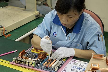
Once the solder joints have cooled, the motherboard is electrically complete. But a final touch needs to be added—the heat sinks for chipsets and MOSFETs. Gigabyte again uses manual labor for this stage. A final check for proper placement of components is also made at this stage.
Now fabrication is complete. Next, the boards have to be tested for proper operation. Gigabyte uses semi-automatic test benches for this. The network connectors, hard disks and CPU cooler are attached to a plate that drops down onto the motherboard in a single movement. Only the daughterboards need to be added. A series of automatic tests is run on the motherboard to test for proper operation of all the components.
Get Tom's Hardware's best news and in-depth reviews, straight to your inbox.
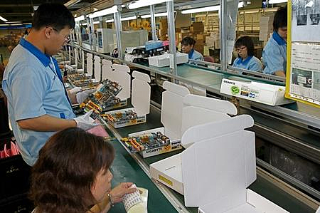
The motherboards that pass all the tests (almost all of them pass) are then sent to the final stage in the fabrication process, packaging. Again, agile human hands place all the items in the box.
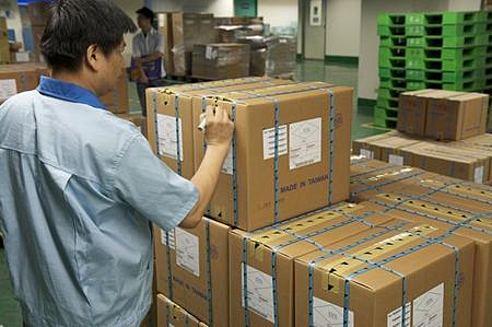
The motherboards or graphics cards are ready, packaged and packed in cartons of 10. They’ll be sent to the United States, Europe, Taiwan, Japan... in short, all over the world.
-
Fadamor Remind me not to buy any Gigabyte products from when those reporters were there. We all know how reporters like to shed! :)Reply -
Mr_Man I couldn't help but notice that with the exception of 3 men in the last 2 pictures, every other employee of Gigabyte seems to be female. I always associate factory jobs with men, but apparently things are different in Taiwan. Of course, it could just be that the photographer "forgot" to take pictures of men.Reply -
pogsnet Wow! you should also visit the other top 3 makers ASUS and MSI. Let's compare them which one is much professional on this. ^_^Reply -
gaiden very insightful. im guessing women workers are on the floor probably because they are more agile with their smaller hands. After all, it's only fair for women to make 'mother'boards i assume :)Reply -
lightfoot__ Wow, that is cool. I have seen wave soldering in person so I know how precise and neat that is. I'm not sure I like how that guy is looking at my DS3L in slide 18 or 19 thought...Reply
Whisper silent... I hope those are earbuds and not earplugs then. I think I'd have some form of carpel tunnel in a week there. Makes me appreciate the boards a bit more.
Thanks for a smart (though not super detailed) write up with fewer then usual errors in the writing! -
Slobogob The Board in picture 17 has a really wicked rear. 4 RJ45 (possibly LAN) connectors and 8 USB? Which Gigabyte board is that?Reply
