The History of Nvidia GPUs: NV1 to Turing
NV1: Nvidia Enters The Market
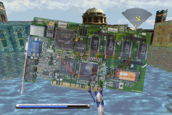
Nvidia formed in 1993 and immediately began work on its first product, the NV1. Taking two years to develop, the NV1 was officially launched in 1995. An innovative chipset for its time, the NV1 was capable of handling both 2D and 3D video, along with included audio processing hardware. Following Sega's decision to use the NV1 inside of its Saturn game console, Nvidia also incorporated support for the Saturn controller, which enabled desktop graphics cards to also use the controller.
A unique aspect of the NV1's graphics accelerator is that it used quadratic surfaces as the most basic geometric primitive. This created difficulties for game designers to add support for the NV1 or to design games for it. This became increasingly problematic when Microsoft released its first revision of the DirectX gaming API, which was designed with polygons as the most basic geometric primitive.
Desktop cards used the common PCI interface with 133 MB/s of bandwidth. Cards could use EDO memory clocked at up to 75 MHz, and the graphics accelerator was capable of a max resolution of 1600x1200 with 16-bit color. Thanks to the combination of Sega Saturn and desktop market sales, Nvidia was able to stay in business, but the NV1 was not particularly successful. Its graphics and audio performance were lackluster, the various hardware components made it expensive compared to other graphics accelerators.
Article continues belowNvidia started work on the NV2 as a successor to the NV1, but after a series of disagreements with Sega, Sega opted to use PowerVR technology inside of its Dreamcast console and the NV2 was cancelled.
MORE: Best Graphics Cards
MORE: Desktop GPU Performance Hierarchy Table
NV3: Riva 128
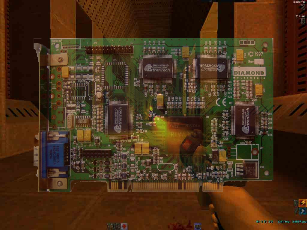
The Riva 128, also known as the NV3, launched in 1997 and was considerably more successful. It switched from using quadrilaterals as the most basic geometric primitive to the far more common polygon. This made it easier to add support for the Riva 128 in games. The GPU also used polygon texture mapping with mixed results. This allowed the GPU to render frames more quickly, but it had reduced image quality.
The GPU was available in two main variants: the Riva 128 and the Riva 128ZX. The Riva 128ZX graphics accelerators used higher-quality binned chips that enabled Nvidia to raise the RAMDAC frequency. Both models used SDRAM memory clocked at 100 MHz accessed over a 128-bit bus, giving the GPUs 1.6 GB/s of bandwidth. The Riva 128ZX chips, however, had 8MB of VRAM compared to 4MB on the Riva 128. The Riva 128ZX also operated at a higher 250 MHz clock speed compared to the Riva 128's 206 MHz.
Get Tom's Hardware's best news and in-depth reviews, straight to your inbox.
These GPUs were fairly popular because they were capable of both 2D and 3D graphics acceleration, though they were clocked lower than alternatives from Nvidia's leading competitor, 3dfx.
NV4: The Plot To Drop The Bomb
In 1998, Nvidia introduced its most explosive card to date, the Riva TNT (code named "NV4"). Similar to the NV3, the NV4 was capable of rendering both 2D and 3D graphics. Nvidia improved over the NV3 by enabling support for 32-bit "True Color," expanding the RAM to 16MB of SDR SDRAM and increasing performance. Although the AGP slot was becoming increasingly popular, a large number of systems didn't contain one, so Nvidia sold the NV4 primarily as a PCI graphics accelerator and produced a relatively small number of AGP-compatible cards. Starting with the Riva TNT, Nvidia made a strong effort to regularly update its drivers in order to improve compatibility and performance.
At the time it was released, 3dfx's Voodoo2 held the performance crown, but it was relatively expensive and was limited to 16-bit color. The Voodoo2 also required a separate 2D video card, which raised its cost of ownership even higher. Needing a separate 2D video card was common in the 1990s, but as the Riva TNT was capable of processing both 2D and 3D video, the card was considerably more budget friendly than the Voodoo2.
Nvidia planned to ship the Riva TNT clocked at 125 MHz in an attempt to take the performance crown from the Voodoo2, but the core simply ran too hot and wasn't sufficiently stable. Instead, Nvidia was forced to ship at 90 MHz with RAM clocked at 110 MHz, resulting in the Riva TNT being slower than the Vodoo2. The Riva TNT still offered decent performance for its time, and after the release of Nvidia's "Detonator" drivers, performance increased significantly making it even more competitive.
Overall the Riva TNT was extremely successful due to its performance and features. The increased driver support from Nvidia also helped to attract customers, as anyone in the 1990s can tell you what a nightmare dealing with drivers used to be.
NV5: Another Explosion
In 1999, Nvidia made another grab for the performance crown with the Riva TNT2 (codenamed "NV5"). The Riva TNT2 was architecturally similar to the original Riva TNT, but thanks to an improved rendering engine it was able to perform about 10 to 17 percent faster than its predecessor at the same clock speed. Nvidia also added support for AGP 4X slots, which provided more bandwidth to the card, and doubled the amount of VRAM to 32MB. Probably the most significant improvement was the transition to 250 nm, which allowed Nvidia to clock the Riva TNT2 up to 175 MHz.
The Riva TNT2's main competitor was the 3dfx Vodoo3. These two products traded blows with each other for years without either card being a clear victor in terms of performance or features.
NV10: Use The GeForce Luke!
In late 1999, Nvidia announced the GeForce 256 (code-named "NV10"). Prior to the GeForce 256, essentially all video cards were referred to as "graphics accelerators" or simply as "video cards," but Nvidia opted to call the GeForce 256 a "GPU." Nvidia packed in several new features with this card including hardware T&L (Transform and Lighting) processing, which allowed the GPU to perform calculations that were typically relegated to the CPU. Since the T&L Engine was fixed-function hardware designed specifically for this task, its throughput was roughly five times higher than a then high-end Pentium III processor clocked at 550 MHz.
The design also differed from the Riva TNT2 in that it contained four pixel pipelines instead of just two. It was unable to match the clock speed of the Riva TNT2, but because of the additional pipelines it was still able to perform roughly 50% faster than its predecessor. The GPU was also Nvidia's first card to use between 32 to 64MB of DDR SDRAM, which contributed to its performance increase. The GPU's transistors shrunk to 220 nm and the core itself operated at 120 MHz, with the RAM ranging from 150 to 166 MHz.
The GeForce 256 also represents the first time Nvidia included video acceleration hardware, but it was limited to motion acceleration for MPEG-2 content.
NV11, NV15, NV16: GeForce2
Nvidia followed the NV10 GeForce 256 up with the GeForce2. The architecture of the GeForce2 was similar to the its predecessor, but Nvidia was able to double the TMUs attached to each pixel pipeline by further shrinking the die with 180 nm transistors. Nvidia used three different cores, codenamed NV11, NV15, and NV16 inside of GeForce2-branded cards. All of these cores used the same architecture, but NV11 contained just two pixel pipelines while the NV15 and NV16 cores had four, and NV16 operated at higher clock rates than NV15.
The GeForce2 was also the first Nvidia line-up to support multiple monitor configurations. GeForce2 GPUs were available with both SDR and DDR memory.
NV20: The GeForce3
In 2001, the GeForce3 (codenamed "NV20") arrived as Nvidia's first DirectX 8-compatible card. The core contained 60 million transistors manufactured at 150 nm, which could be clocked up to 250 MHz. Nvidia introduced a new memory subsystem on the GeForce3 called "Lightspeed Memory Architecture" (LMA), which was designed to compress the Z-buffer and reduce the overall demand on the memory's limited bandwidth. It was also designed to accelerate FSAA using a special algorithm called "Quincunx." Overall performance was higher than the GeForce2, but due to the complexity of the GPU it was fairly expensive to produce, and thus carried a high price tag in comparison.
NV2A: Nvidia And The Xbox
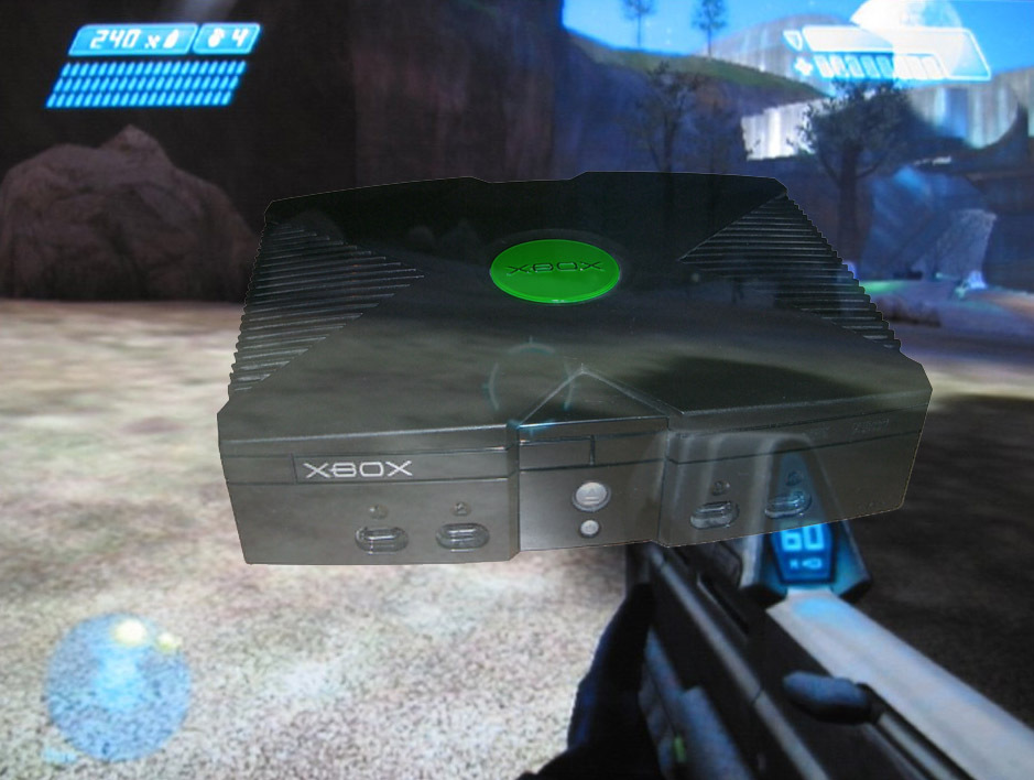
Nvidia would once again find itself back in the home console market as a key component of Microsoft's original Xbox in 2001. The Xbox used hardware nearly identical to what you would find inside of modern PCs at that time, and the GPU designed by Nvidia was essentially a tweaked GeForce3. Just like the NV20 GPU, the NV2A inside of the Xbox contained four pixel pipelines with two TMUs each. Nvidia also created the Xbox's audio hardware known as MCPX, or "SoundStorm".
NV17: GeForce4 (Part 1)
Nvidia started to shake things up in 2002 by introducing several GPUs based on different architectures. All of these were branded as GeForce4. At the low-end of the GeForce4 stack was the NV17, which was essentially an NV11 GeForce2 die that had been shrunk using 150 nm transistors and clocked between 250 and 300 MHz. It was a drastically simpler design compared to the NV20, which made it an affordable product that Nvidia could push to both mobile and desktop markets.
Nvidia later released two revisions of the NV17 core called NV18 and NV19. NV18 featured an upgraded bus to AGP 8X, while NV19 was essentially an NV18 chip with a PCIe bridge to support x16 links. The DDR memory on these chips was clocked anywhere between 166 and 667 MHz.
NV25: GeForce4 (Part 2)
With the NV17 covering the lower-half of the market, Nvidia launched NV25 to cover the high-end. The NV25 was developed as an improvement upon the GeForce3's architecture, and essentially had the same resources with four pixel pipelines, eight TMUs, and four ROPs. The NV25 did have twice as many vertex shaders (an increase from one to two), however, and it featured the updated LMA-II system. Overall, the NV25 contained 63 million transistors, just 3 million more than the GeForce3. The GeForce4 NV25 also had a clock speed advantage over the GeForce3, ranging between 225 and 300 MHz. The 128MB DDR memory was clocked between 500 to 650 MHz.
Benchmarks of the NV25 in DirectX 7 titles showed modest performance gains over the GeForce3 of around 10%. However, DirectX 8 games that took advantage of the vertex shaders saw the performance advantage held by the NV25 grow to 38%.
Nvidia later released a revised NV25 chip, called the NV28. Similar to the NV18 mentioned in the last slide, the NV28 only differed from the NV25 in that it supported AGP 8X.
MORE: How Well Do Workstation Graphics Cards Play Games?
NV30: The FX 5000 (Part 1)
In 2002, the gaming world welcomed the arrival of Microsoft's DirectX 9 API, which was one of the most heavily used and influential gaming APIs for several years. ATI and Nvidia both scrambled to develop DX9-compliant hardware, which meant the new GPUs had to support Pixel Shader 2.0. ATI beat Nvidia to the market in August 2002 with its first DX9-capable cards, but by the end of 2002 Nvidia launched its FX 5000 series.
Although Nvidia launched its DX 9 cards later than ATI, they came with a few additional features that Nvidia used to attract game developers. The key difference was the use of Pixel Shader 2.0A, Nvidia's own in-house revision. Pixel Shader 2.0A featured a number of improvements over Microsoft's Pixel Shader 2.0, such as unlimited dependent textures, a sharp increase in the number of instruction slots, instruction predication hardware, and support for more advanced gradient effects. Essentially, Pixel Shader 2.0A contained several improvements that would become part of Microsoft's Pixel Shader 3.0.
Crafted using 130 nm transistors, NV30 operated between 400 and 500 MHz, and it had access to 128 or 256MB of DDR2 RAM over a 128-bit bus operating at either 800 or 1000 MHz. The NV30 itself continued to use a four-pipeline design with two vertex shaders, eight TMUs, and four ROPs. Nvidia followed it up with lower-end variants that had four pixel pipelines and just one vertex shader, four TMUs, and four ROPs and could use less expensive DDR memory.
-
abryant Archived comments are found here: http://www.tomshardware.com/forum/id-3407581/history-nvidia-gpus.htmlReply -
kinggremlin So, based on the archived comments, this is the THIRD time this article has been posted since the release of Pascal. Why on earth would you keep recycling this article when nothing has been added to the "history?" Turing has not been released yet, we have no benchmarks. Unless this site has no intention of posting reviews of the Turing cards, there is zero reason to re-re-post this just to add an unreleased architecture on the last slide with no useful or new information.Reply -
bit_user Anyone interested in early GPUs (particularly Nvidia's exotic NV1 and its cancelled successor) would probably find this a worthwhile read:Reply
http://vintage3d.org/nv1.php#sthash.AWlq2ihY.dpbs
He thoroughly explores their unique quadric rendering approach, including its down-sides and how they tried to mitigate.
The author of that site has posted on here, in a previous article about vintage 3D cards. Maybe he'll show up, again. -
Blytz I really love to see a graph of the processing power and memory bandwidth of the evolution of these cards (and throw in the ati/radeons as well) to see when we made leaps or increments and how far it's all come.Reply -
bit_user Reply
This isn't exactly relevant to graphics performance, but still worth a look.21265764 said:I really love to see a graph of the processing power and memory bandwidth of the evolution of these cards (and throw in the ati/radeons as well) to see when we made leaps or increments and how far it's all come.
https://www.karlrupp.net/2013/06/cpu-gpu-and-mic-hardware-characteristics-over-time/
Note that the Y-axis of most plots is in log-scale. Also, even though it's from 2013, he updated it for KNL and Pascal. I just wish he'd update it with Volta.
Edit: If you liked that, you might enjoy his 42 Years of Microprocessor Trend Data. -
Unsal Ersoz Wow, I was a very hardcore gamer back then :)Reply
TNT2 and Voodoo3 were competitors until 3DFX released its January 2000 drivers. I can remember it like yesterday. That miniGL port for the opengl games like half-life, quake and others that is long forgotten basically blew tnt2 to the dust (I owned both of the hardware). At 2000, Nvidia was very incompetitive from the software perspective compared to 3dfx with voodoo3. I remember my GLquake renders 10720fps timelapse while tnt2 was stuck with ~60ish :)
Nice memories. -
samopa I am in 3dfx camp until I had forced to switch to nVidia camp. I owned Voodoo1, Banshee, Voodoo2, Voodoo3 3000, Voodoo5 5500 before finally switch to GeForce 6800 Ultra.Reply
Such a fond memories -
AgentLozen I remember posting a comment on this article the last time it came around.Reply
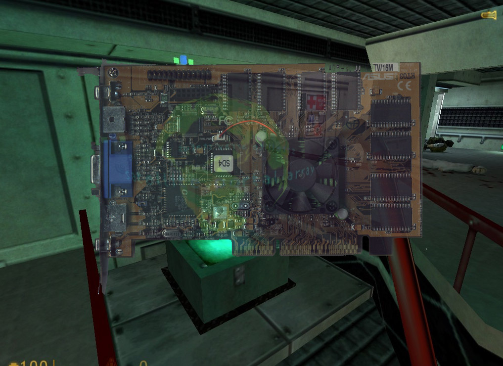
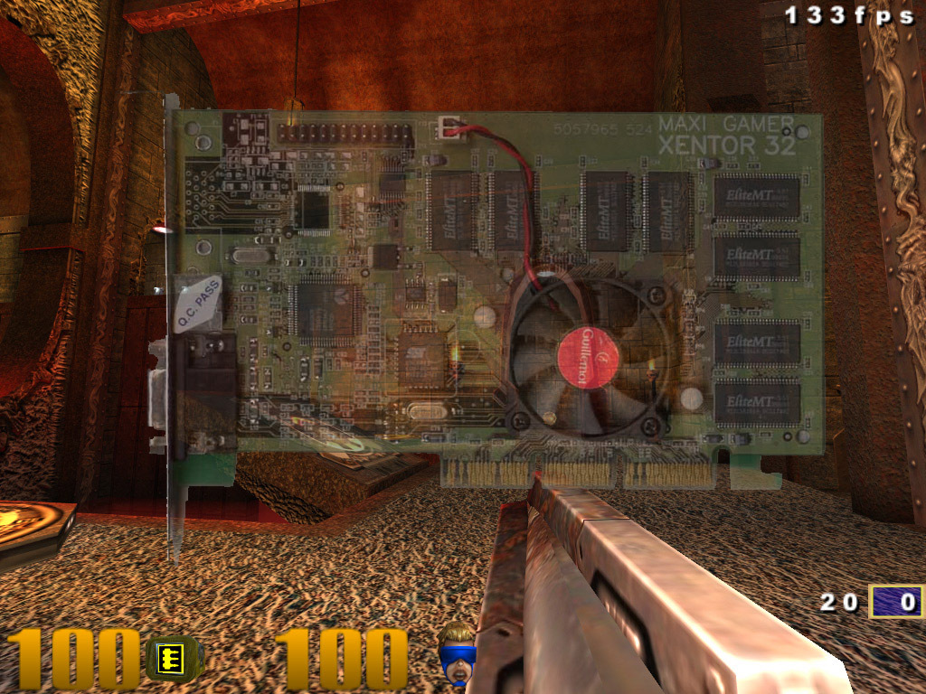
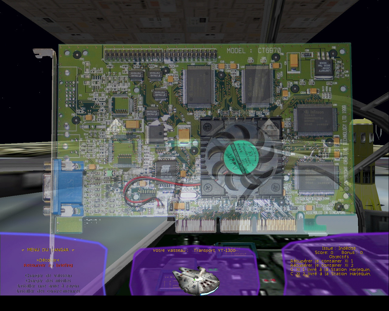
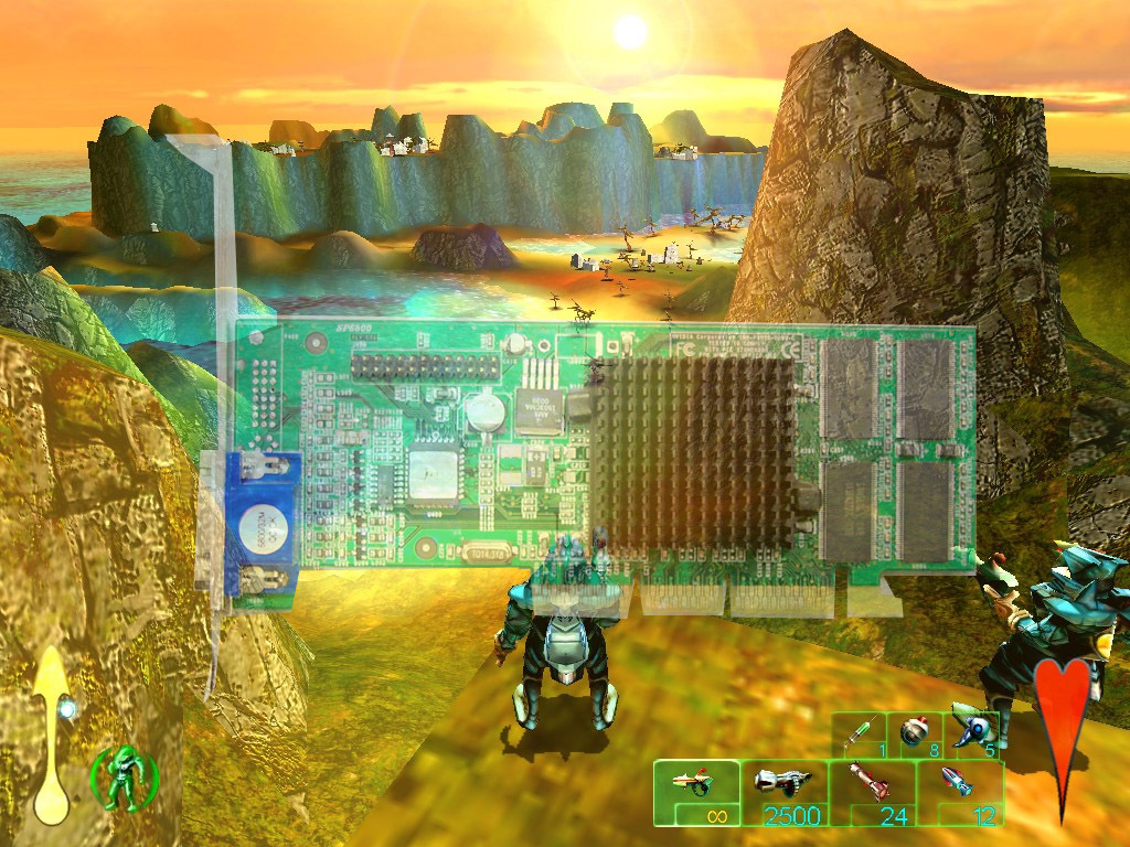
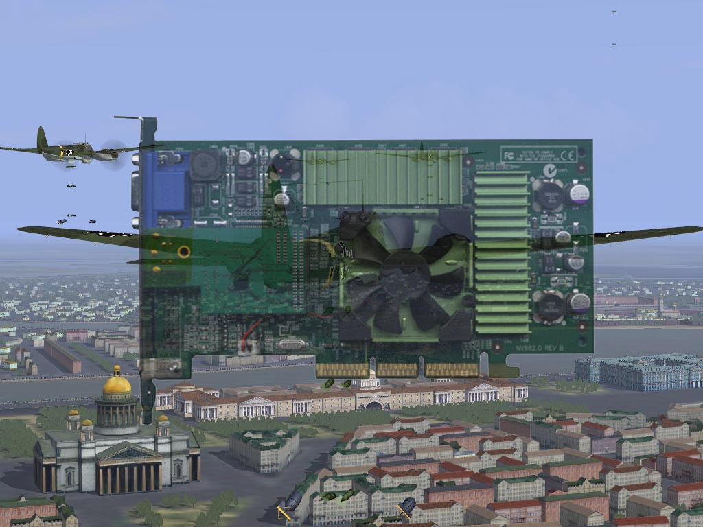
I mentioned last time that I liked the video game screenshots in the background. It helps put the hardware into perspective. For example, the TNT was meant to play games like Half Life. The TNT2 was built to take on Quake 3.
My unique contribution this time is that I would like to see the date of each card's release on each slide. Some entries have this and others don't. I mentioned perspective in my last paragraph and the same applies here. A good analogy for why the date is important would be like taking a history class and hearing "In 1941, America entered World War 2. A short time later, America found itself in Vietnam." So...... was America in Vietnam in that same decade? In the 1950's? The 1960's? It would help my understanding to have a date.
I did enjoy reading this article even if I've looked at it before. -
Stephen_144 The 3dfx was my second gfx card. My second computer, a Pentium 90, had a Diamond Viper Stealth card which I later upgraded to a 3DFX.Reply
I recall loading Windows for Work groups because I could get a 800x600 resolution all the way up to 256 colors. That was up from 640x480 16 colors in the regular windows 3.0. I recall being amazing all the images and spent the entire day downloading (from my dial up Comp-u-Serve 28k modem) color icons and customizing all my windows to use them. Awww simpler times. -
steve.d.moss Is this another biased article like the one telling us to buy RTX cards without even waiting for concrete proof of performance and at inflated prices? I really hope not.Reply
The history of Nvidias rise to power is far more convoluted and full of lies, skullduggery and deceit than people realise.
Check out Adored TV on YouTube. He did a totally unbiased and crystal clear video on this topic a few months back.
Definitely worth a watch, might even open your eye a little.
