The 30 Year History of AMD Graphics, In Pictures
ATI Radeon HD 2900 XT (2007)
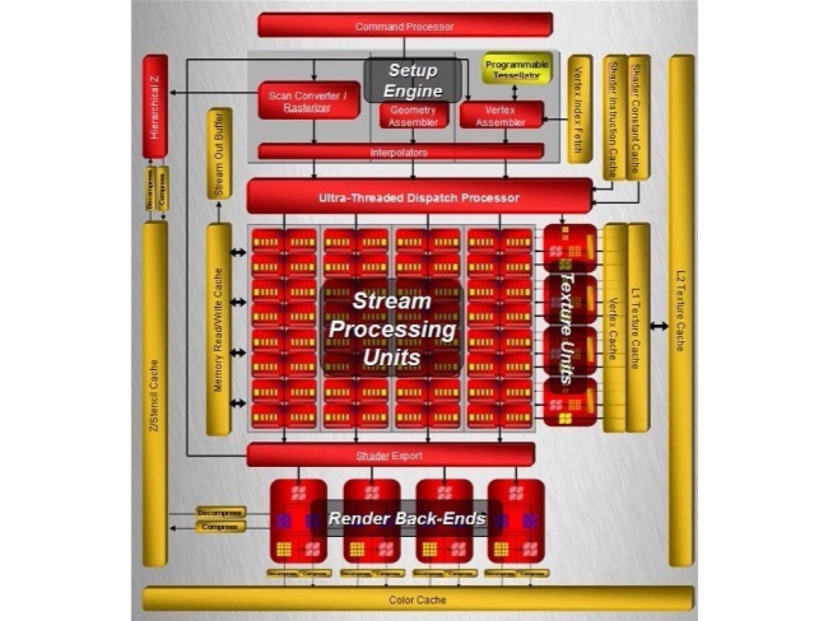
ATI introduced an almost entirely new architecture called TeraScale to power its Radeon HD 2000-series products. This was ATI's first unified shader architecture, and it was also the first design introduced after ATI's merger with AMD. TeraScale was designed to be fully compatible with Pixel Shader 4.0 and Microsoft's DirectX 10.0 API. It first appeared inside of the R600 core, which powered the Radeon HD 2900 XT flagship.
The Radeon HD 2900 XT included similar video acceleration features as AMD's older GPUs. This was done in part to reduce the overall production costs of the chip, but also because the CPUs of the time were fast enough to handle media decoding, albeit at higher power consumption.
Although the new card's architecture differed significantly from AMD's Radeon X1000 series, one key element shared between them was the ultra threaded dispatch processor mentioned on the previous page. However, it was updated to increase performance and efficiency. The R600 GPU was manufactured on an 80 nm process, and it had a total of 320 Stream processors, 16 TMUs, and 16 ROPs. The core continued to use a ring bus, in this case populated by eight 64-bit memory controllers connected to 512 MB of GDDR3 or 1 GB of GDDR4.
The Radeon HD 2900 XT performed well, but it was unable to match Nvidia's flagship GeForce 8800 GTX.
ATI Radeon HD 3870 (2007)
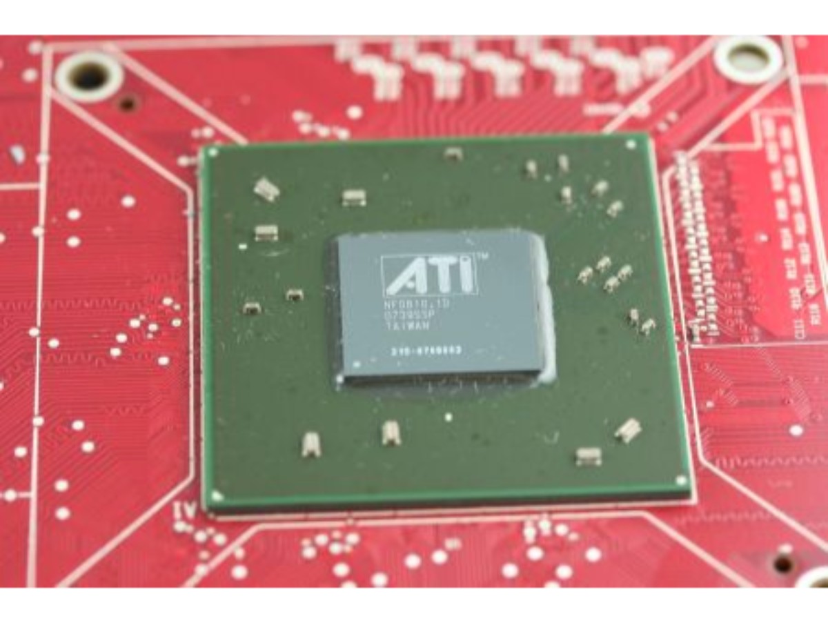
Later in 2007, ATI introduced its Radeon HD 3870. This successor to the Radeon HD 2900 XT used essentially the exact same design, but transitioned to 55 nm manufacturing. AMD also optimized the memory interface and upgraded to PCIe 2.0. The most notable addition to the 3870's R670 GPU was UVD, ATI's hardware-accelerated video decode engine.
ATI gave the Radeon HD 3870 a higher clock rate, yielding a performance advantage over the previous generation. But it was not significantly faster.
ATI Radeon HD 4870 (2008)
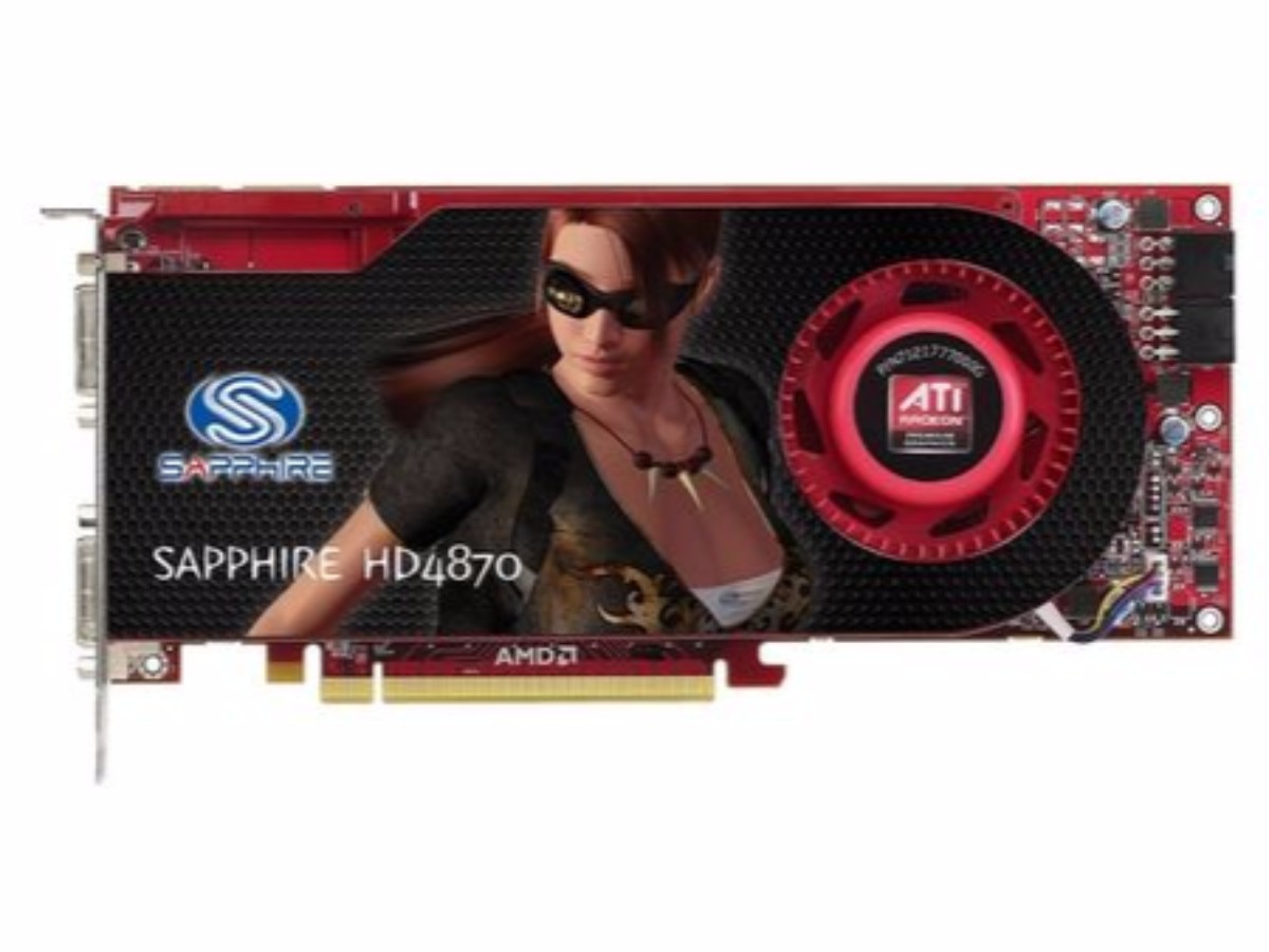
As ATI's Radeon HD 2900 XT and Radeon HD 3870 were unable to compete with Nvidia's latest, the company desperately needed a new high-end GPU. This came in 2008 in the form of the RV770, inside of its Radeon HD 4870 utilizing the same architecture as its predecessor on a 55 nm process. The core had 800 Stream processors, 40 TMUs, and 16 ROPs connected to either 512 MB or 1 GB of memory on a 256-bit bus. Since GDDR5 was relatively new at the time, it only operated at 900 MHz. Still, this gave the Radeon HD 4870 an abundance of memory bandwidth.
Stay On the Cutting Edge: Get the Tom's Hardware Newsletter
Get Tom's Hardware's best news and in-depth reviews, straight to your inbox.
The GPU was clocked roughly the same as the Radeon HD 3870 at 750 MHz, but due to the added execution resources and steep increase in memory bandwidth, the Radeon HD 4870 was quite a bit faster. It couldn't catch Nvidia's GeForce GTX 280, but was significantly less expensive and highly competitive for its time. It also marked ATI's return to the high-end GPU market.
ATI Radeon HD 4890 (2009)
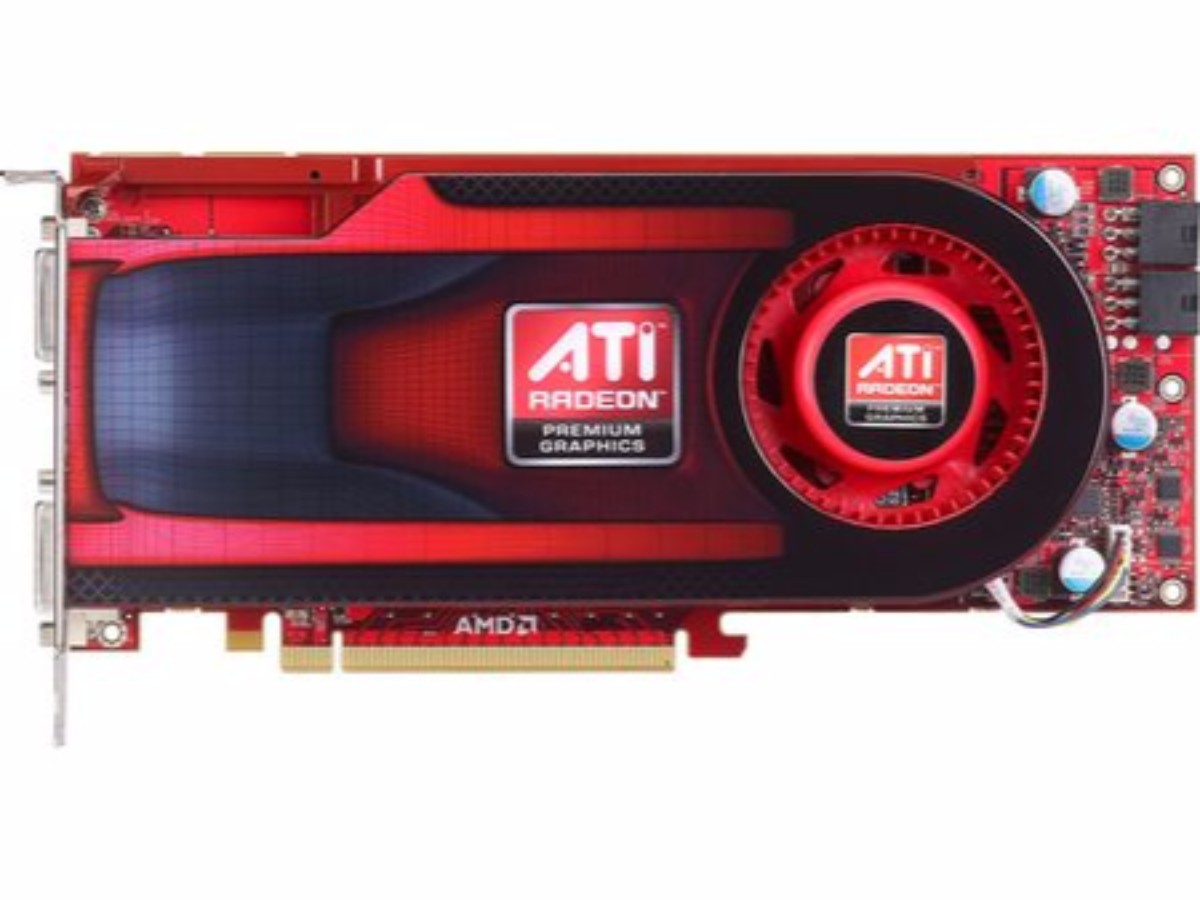
ATI went through the RV770 die and tweaked it to facilitate higher clock rates, resulting in the Radeon HD 4890's RV790 GPU. This card was clocked 100 MHz faster than the Radeon HD 4870, but was otherwise identical. Performance increased, if only slightly.
ATI Radeon HD 5870 (2009)
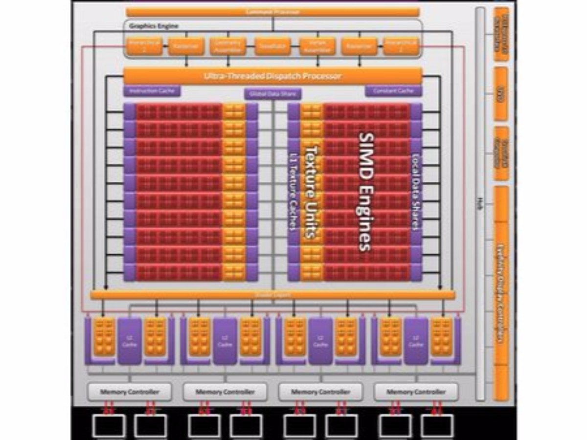
The Radeon HD 4890 didn't sit on top of ATI's product line-up for long, as the company launched its Radeon HD 5870 later the same year. It used a new TeraScale II architecture designed to support DirectX 11. A key improvement moving from TeraScale to TeraScale II was that the individual Stream processors were capable of handling a wider array of instructions.
The Cypress core inside of Radeon HD 5870 had 1600 Stream processors, 80 TMUs, and 32 ROPs. The Radeon HD 5870 operated at 850 MHz, and it connected to 1 GB of GDDR5 over a 256-bit interface. The core was etched using 40 nm transistors, which helped reduce power consumption despite the more complex GPU. Overall, the Radeon HD 5870 was nearly twice as fast as its predecessor, and for a time it claimed the performance crown as the fastest GPU in the world.
AMD Radeon HD 6970 (2010)
AMD acquired ATI back in 2006, but continued to use ATI's brand until the introduction of the Radeon HD 6000 series.
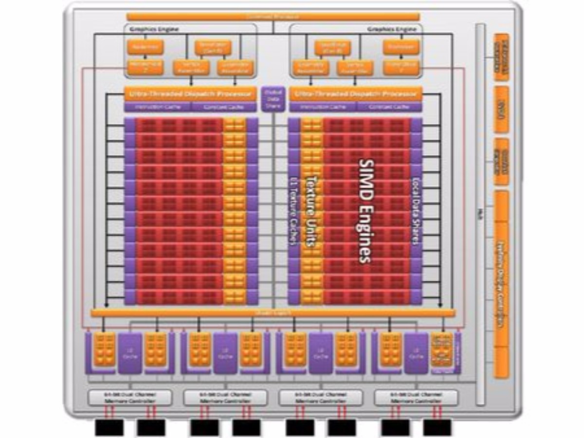
The company realized that the Cypress GPU was incapable of keeping the Stream processors adequately fed. This was inefficient, as all of the cores were powered, but some were idle. The solution was to reduce the number of Stream processors slightly, which resulted in an increase in efficiency and GPU utilization. AMD then added new SIMD engines, though the end result was a 6000-series with fewer resources than its predecessor. This architecture became known as TeraScale 3.
The 6000-series flagship, AMD's Radeon HD 6970, shipped with 1536 Stream processors, 96 TMUs, and 32 ROPs. The 6970's Cypress GPU was manufactured using 40 nm transistors. It also used the same 256-bit bus, but had access to 2 GB of GDDR5. The architectural improvements allowed the 6970 to outperform AMD's previous effort while also being more energy efficient overall.
AMD Radeon HD 7970 (2011)
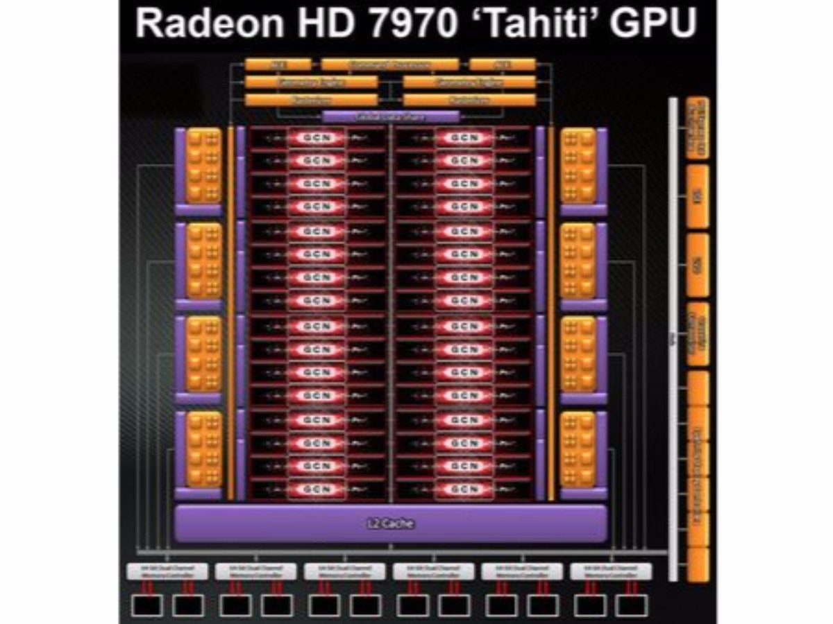
In 2011, AMD left its TeraScale architecture behind in favor of Graphics Core Next, completely re-designed and based on a RISC microarchitecture. One of the company's goals was a processor well-suited for gaming and GPGPU work. As a result, the Radeon HD 7970 saw a sharper increase in compute performance than almost any other discipline. GCN first appeared inside of AMD's Radeon HD 7000-series graphics cards. The flagship Radeon HD 7970 sported 2048 Stream processors, 128 TMUs, and 32 ROPs built with 28 nm transistors. Even with the increase in resources, the Radeon HD 7970's Tahiti GPU was more compact and able to attain higher clock rates than its predecessor. The Radeon HD 7970 launched at 925 MHz, with access to 3 GB of GDDR5 on a 384-bit bus.
The Radeon HD 7970 outperformed all other single-GPU graphics cards by a wide margin. In some games, it was able to beat dual-GPU cards like the Radeon HD 6990 and GeForce GTX 590 as well. It consumed more power than its predecessor, though.
AMD Radeon HD 7970 GHz Edition (2011)
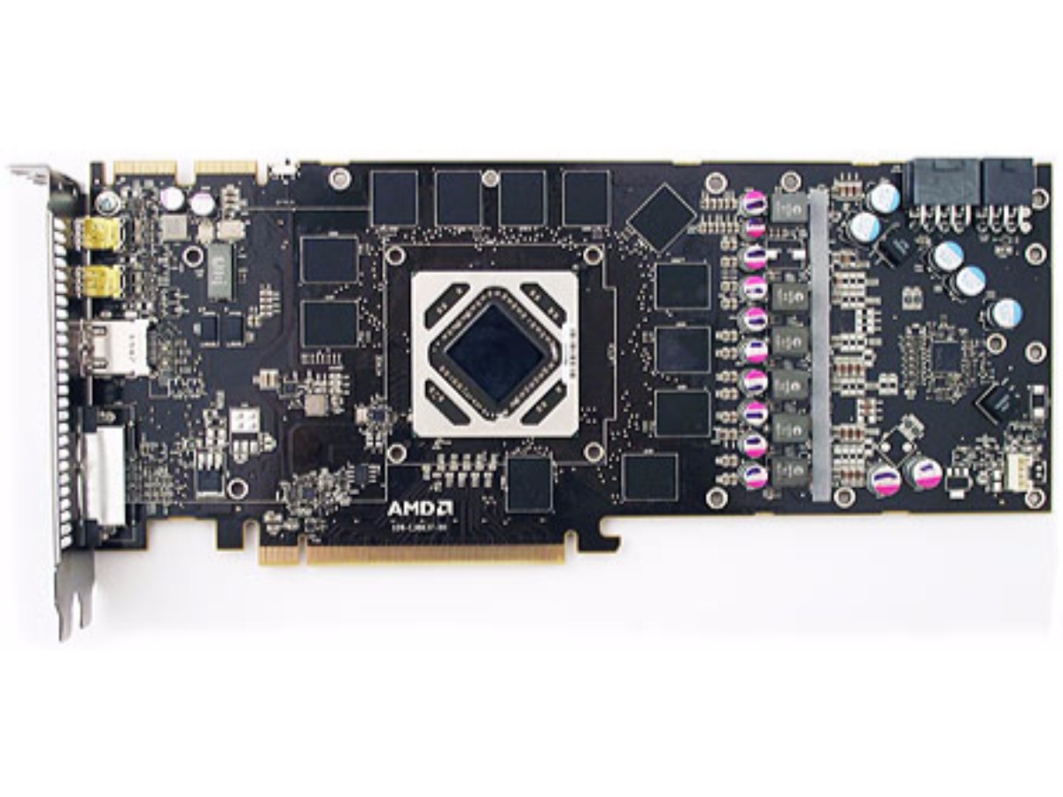
Following the release of the Radeon HD 7970, Nvidia fired back with its GeForce GTX 680, which was slightly faster. AMD responded by pushing up the clock rate on Tahiti to 1000 MHz, creating the Radeon HD 7970 GHz Edition. It also introduced AMD's Boost feature, and in certain situations the card jumped to 1050 MHz. AMD also pushed up its memory clock to 6 GT/s. Those specifications allowed AMD's Radeon HD 7970 GHz Edition to match and sometimes surpass the GeForce GTX 680.
AMD Radeon HD 8000 Series
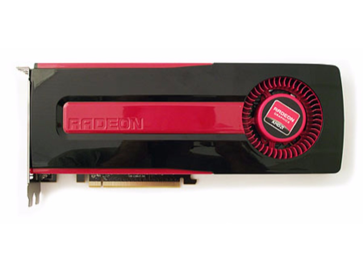
AMD's Radeon HD 8000 series was made up entirely of rebadged cards. Most of them came from the 7000 series and were based on the GCN architecture, but a few drew from the older TeraScale design.
AMD Radeon R9 290X (2013)
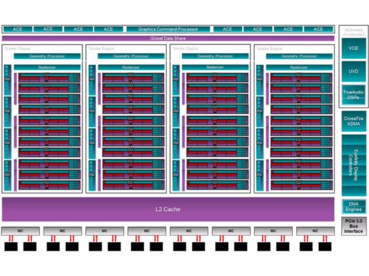
AMD's Radeon HD 7970 GHz Edition was one of the company's longest-standing flagships. Eventually, it was replaced by the Radeon R9 290X and its Hawaii GPU, which was manufactured using the same 28 nm lithography and based on an updated version of GCN. The size of the L2 cache increased from 768 KB to 1 MB, and AMD improved bandwidth between on-die resources. AMD also introduced its TrueAudio technology, leveraging DSP cores to accelerate audio processing in optimized software.
The Hawaii GPU contained 2816 Stream processors, 176 TMUs, and 64 ROPs connected to 4GB of GDDR5 over a 512-bit bus. The R9 290X was undeniably fast, often outperforming Nvidia's GeForce GTX Titan and GeForce GTX 780. The reference card wasn't perfect, however, as it had serious heat issues that imposed lower clock rates in order to run within its thermal specifications. You could manually set the fan speed higher, though this made the stock thermal solution loud and bothersome. This issue largely vanished after AMD's board partners produced versions of the R9 290X with more efficient coolers, however, and the R9 290X was able to hold the performance crown for awhile.
-
adamovera Archived comments are found here: http://www.tomshardware.com/forum/id-3207492/year-history-amd-graphics-pictures.htmlReply -
XaveT I still have a 5870 in production. Great card. And six miniDP ports on one card is great for the workstation it's in. I'm sad to see no current flagships with the same configuration, I may have to do two graphics cards or get an unneeded professional series card at upgrade time.Reply -
Nuckles_56 This sentence doesn't make a lot of senseReply
"All-in-Wonder 8500 close to the performance of AMD's Radeon 8500, which was enough to compete against Nvidia's GeForce 3." -
cub_fanatic I have a couple of those 8500 all-in-wonder cards with the remote, receiver for the remote, the giant dongle, the software and all. A friend had them sitting in his garage and was going to chuck them so I took them home. I believe they were used in a doctor's office or something so that they could have a single display in the room and switch to TV while the patient waited and then back to a desktop to show them x-rays or whatever. I have one hooked up to a Pentium 4 Dell running XP but can't figure out much of a use for it in 2017. Even the tuner is almost useless unless you want to capture a video off of a VCR since they can only handle analog.Reply -
Martell1977 My first ATI discreet GPU was a Radeon 9250, and it was pretty good at the time considering the resolutions of the CRT monitors. My second was a Radeon 3850 AGP, while my brother went with a nVidia card. I sold the 3850 with the other parts, working, on eBay mid last year....my brothers nVidia card barely outlasted the warranty.Reply
Next came my 6870, which I got in 2010 and tried crossfire in 2015, but ended up upgrading to a R9 390 as the 6870's ran into memory issues.
I know a lot of people complain about AMD/ATI drivers, but I've had more issues with nVidia driver (especially recently) than any AMD. Both my laptops have been nVidia GPU's (8600M GT and 1060 3gb).
Awaiting to see what Vega brings, I'm surprised it didn't at least get a tease at the end of the article, but hey, maybe this is a lead up to a Vega release soon? -
I look forward to the next 30 years.Reply
P.S. Maybe eventually heterogeneous compute will work. I doubt it. In any case, they seem back in formation, and charging forward. -
blackmagnum I hate reading this page format on IOS; lots of problems and hangs with page scrolling.Reply -
CRO5513Y You can definitely see the change in Aesthetics, what ever happened to all the fancy details and characters on the cards? :PReply
(I mean to be fair not much room to fit them on cards these days since most have non-blower style coolers). -
LaminarFlow Hard to believe that I've been an ATI user for almost 15 years now. Always had a somewhat limited budget, I picked up a 9600XT in 2003, then X1900 XT in 2006, HD 4850 in 2008 (for $125, that was the best computer part purchased I ever made), and R9 280X in 2013.Reply