AMD A10-7850K And A8-7600: Kaveri Gives Us A Taste Of HSA
We've spent the days following CES benchmarking two of AMD's new Kaveri-based APUs. Do the Steamroller x86 architecture, GCN graphics design, and HSA-oriented features impress, or do they come up short against Intel's value-oriented Haswell-based parts?
Meet The Compute Core
Send In The Marketers
Here’s the part of the discussion where our more technical readers may let out a collective groan. Last generation, AMD referred to its x86 and graphics shaders independently. A10-6800K had four cores (actually, two Piledriver modules with four distinct integer clusters) and 384 shaders.
This time around, the company takes the fundamental graphics building block—the Compute Unit—which is replicated over and over to give us GCN-based GPUs like Hawaii with up to 2816 shaders, and dubs it a Compute Core. By definition, a Compute Core is HSA-enabled, programmable, and capable of running at least one process in its own context and virtual memory space, independent of other cores.
Of course, this gives AMD the ability to sum its CPU and GPU resources, yielding Kaveri-based APUs with eight and 12 compute cores, all with access to the same unified coherent memory. That’s compelling nomenclature when your competition is selling dual- and quad-core mainstream processors. Fortunately, the company’s legal department insists on a specific breakdown of CPU and GPU resources any time core count is used to describe a Kaveri-based APU.
Article continues belowAMD (validly) posits that it wants the technical community to think of up to 12 threads running concurrently, which is why it talks about Kaveri as a 12-core device. The APU does, in fact, address parallelism in a new and interesting way. We simply want to see the company use its messaging for good. At a time when AMD talks about CPUs in terms of their highest Turbo Core frequencies and rates high-end GPUs for clock rates they simply cannot sustain, the mainstream customers most likely to buy an APU aren’t going to understand the advanced implications of its nomenclature.
A New x86 Architecture: The First Steamroller CPU
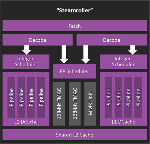
At least most folks seem comfortable with the definition of AMD’s module-based approach to x86 cores, right? Kaveri represents the first outing for the Steamroller architecture, succeeding the Piledriver design at the heart of AMD’s Richland APUs. Although some of those previous-gen parts sported one module (or two cores), the just-introduced Kaveri models include two. AMD calls this a four-core configuration, though we know each module exposes two integer clusters and a shared floating-point unit.
Back when AMD introduced the Bulldozer architecture, we immediately took note of the big step back in per-cycle performance. Piledriver helped a little, but IPC remained painfully low compared to Intel’s Sandy Bridge, Ivy Bridge, and Haswell architectures. Steamroller was designed to help make up some of the difference, and engineers claim instruction throughput is up as much as 20%. Unfortunately, manufacturing decisions temper that gain.
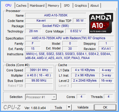
The changes made to Steamroller predominantly improve efficiencies at the front-end of the pipe to minimize stalls and, according to AMD, get single-threaded performance back up to more competitive levels. The L1 instruction cache, previously 64 KB and two-way set associative, is now 96 KB and three-way set associative, reducing misses by 30%. AMD’s engineers similarly went after mispredicted branches by increasing the L2 branch target buffer from 5000 to 10,000 entries and augmenting the branch predictor itself. Instruction scheduling is made 5 to 10% more efficient through a jump to 48 entries (from 40). And company reps say that both integer clusters can access the microcode ROM simultaneously now, where they couldn’t before. Steamroller can issue two stores at once; the Piledriver architecture would only do one. Finally, the load/store units in each integer cluster feature ~20%-larger queues, further benefiting efficiency.
Get Tom's Hardware's best news and in-depth reviews, straight to your inbox.
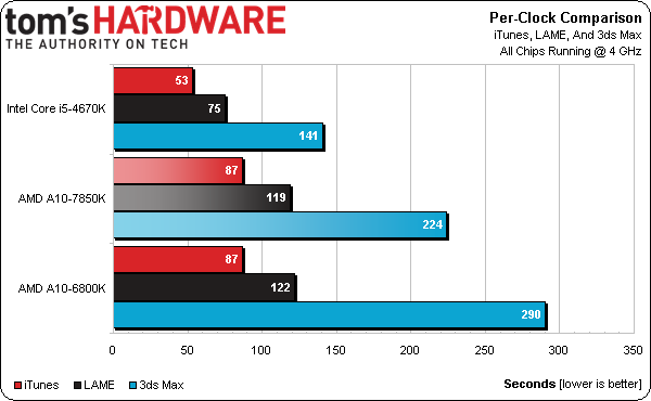
To test AMD’s claims, I dialed in a Core i5-4670K, A10-6800K, and A10-7850K to exactly 4 GHz, then ran our single-threaded iTunes and LAME benchmarks.
In iTunes, Steamroller gets exactly zero benefit. The Haswell-based Core i5 is naturally quite a bit faster. LAME actually reflects a tiny gain, but again, Intel’s architecture enjoys a commanding lead.
Frustrated at the lack of single-core speed-up, I decided to add our threaded 3ds Max 2013 render project. Only then, after spinning up both Steamroller modules, does the architecture demonstrate significantly better results. At 4 GHz, the A10-7850K is 22% faster than the A10-6800K. Some of that is eroded in practice by the Richland-based APU’s higher shipping clocks. However, it does appear that improvements made to Steamroller show up selectively, depending on the workload.
Current page: Meet The Compute Core
Prev Page Steamroller, GCN, HSA, 28 nm: Oh My! Next Page A More Capable GPU: GCN Surfaces In Kaveri-
Someone Somewhere Yeah, almost all the diagrams refer to the 4760K.Reply
Given that AM3+ looks like it's done, it would have been nice to see a 6-core chip. Still, one of these may end up in my next laptop. -
spp85 A10-7850k is slower than A10-6800K ?? WTF. Its all hype than actual performance to the table. Even on OpenCL GPU accelerated apps doesn't have any advantage with A10-7850k over i5 or sometimes i3 CPUs. Hopeless is what I feel about AMD CPUs.Reply -
Someone Somewhere Reply12454254 said:A10-7850k is slower than A10-6800K ?? WTF.
I got the opposite impression. Which graph are you looking at? -
Jaroslav Jandek Thank you for the article (especially the power consumption measurements), Chris. It is definitely an improvement over Richland but kind of boring (disappointingly expectable).Reply
I really like where AMD is going (HSA, GCN and TrueAudio).Too bad the manufacturing process of GlobalFoundries just can't match Intel's.
Also, it would be interesting to see the new Bay Trail Pentium or Celeron CPUs (whichever is closer in performance) in the Efficiency graphs. -
Someone Somewhere I'm fairly sure that this is on TSMC's 28nm node. GlobalFoundries can't do that yet; this is on the same process used for AMD GPUs currently.Reply -
Jaroslav Jandek Reply
28nm SHP from GlobalFoundries. AMD bought over $1 billion worth of wafers from them in december...12454280 said:I'm fairly sure that this is on TSMC's 28nm node. GlobalFoundries can't do that yet; this is on the same process used for AMD GPUs currently.
I guess you have been reading the articles from a year ago about AMD still using TSMC despite promises of GlobalFoundries' new 28nm SHP process. -
jacobian I don't really believe into the whole HSA smoke-screen. By the time HSA-enabled apps take off, you will be ready to upgrade from your CPU again. The one terrible truth that stands out right now is that at current prices, the flagship Kaveri A10 doesn't make any sense whatsoever. Kaveri A8? Maybe. Richland A10-6790K? Perhaps. But the Kaveri A10 at $180 is a just a joke, specially after all that hype.Reply -
Someone Somewhere CPUs are usually released at ridiculous prices, and come down over a month or two.Reply


