Future Promise for Graphics: PCI Express
Get Tom's Hardware's best news and in-depth reviews, straight to your inbox.
You are now subscribed
Your newsletter sign-up was successful
Bridge It - NVIDIA's HSI Bridge, Continued
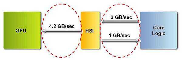
Nonetheless, there are some real problems that can crop up when a PCIe -> AGP bridge is used. Firstly, there is the matter of the "low" AGP bandwidth between the HSI chip and the graphics processor. When a sufficiently bandwidth-hungry application is used, the AGP link could theoretically become a bottleneck. However, since the HSI chip sits directly on the graphics card, the signal length to the graphics chip is very short. Since there is no AGP slot with a motherboard behind it, the engineers can work with much higher tolerances. Through some additional design work on the circuit board, NVIDIA was able to increase the peak (!) AGP bandwidth to AGP 12x (3.1 GB/s) for the entry-level PCX models and to AGP 16x (4,2 GB/s) for the high-end models. That makes AGP on PCX cards as a bottleneck a moot point - at least in theory.
Diagram of NVIDIAs HIS architecture used by the new GeForce PCX models.
Another disadvantage of any bridge solution are latencies. These arise from the fact that the signals have to be translated, which takes time. NVIDIA's answer to this is that the graphics processor expects certain delays anyway, generated by the AGP bus and the motherboard chipset. According to NVIDIA, the latencies generated by the HSI chip are well within these tolerances. This is because NVIDIA graphics processors request data packets of 64Bits (request size). NVIDIA goes on to explain that the request size of other (not NVIDIA = ATi?) graphics chips is only 32Bits, with lower latency tolerances. Could this be an innuendo that ATi wouldn't be able to use a bridge chip anyway, even if it wanted to.
Article continues belowThe bridge in use.
Get Tom's Hardware's best news and in-depth reviews, straight to your inbox.
Current page: Bridge It - NVIDIA's HSI Bridge, Continued
Prev Page Bridge It - NVIDIA's HSI Bridge Next Page Bridge It - NVIDIA's HSI Bridge, Continued
