GeForceFX: NVIDIA goes Hollywood?
Get Tom's Hardware's best news and in-depth reviews, straight to your inbox.
You are now subscribed
Your newsletter sign-up was successful
The Chip
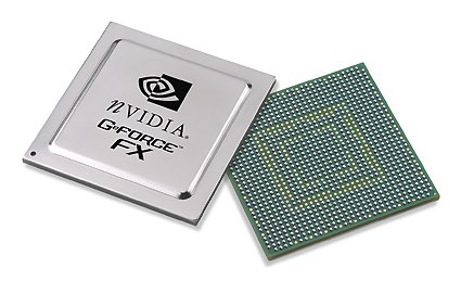
The GeForceFX, alias NV30, is the first NVIDIA chip designed using technologies gained through the acquisition of 3dfx and Gigapixel. The chip itself is a completely new design that has very little in common with the GeForce4 Ti.
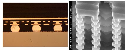
The GeForceFX chip will be produced on TSMC's 0.13µ process, making it the first consumer 3D chip ever to use this process. Compared to the current 0.15 microns, the new design shrinks the transistors by 25% and makes them 25% faster. Power consumption is also reduced by a full 36% according to NVIDIA. However, the biggest advantage lies in the higher clock speeds such a design allows. The flip-chip design is a contributing factor here, since the gates can be flush against their contact pins. Older designs use traces that connected the chip to these contacts, making them more susceptible to signal noise.
Left: Flip-Chip Design - Right: X-ray of the transistors
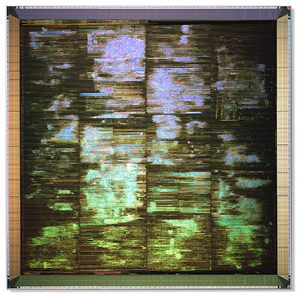
With this new, highly scalable design, NVIDIA feels prepared to face the future, even where production costs are concerned. Although NV30 consists of roughly 25 million more transistors than ATi's R300, the resulting die should end up being roughly the same size, if not smaller.
A die-shot of the GeForceFX.
Get Tom's Hardware's best news and in-depth reviews, straight to your inbox.


