Semiconductor Production 101
Get Tom's Hardware's best news and in-depth reviews, straight to your inbox.
You are now subscribed
Your newsletter sign-up was successful
Wafer Fabrication
The first part of processor manufacturing has to be performed in a clean room area and I believe it is important to say that this type of technology introduces one of the highest capital densities per square foot. Building up a modern fab with all the equipment easily costs $2-$3 billion dollars, and it takes several months of test runs with new technology before a new fab can output silicon for mass producing processors.
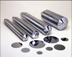
In short, the manufacturing process consists of a series of wafer processing steps. These steps include creating wafer ingots, which are cut into slices to go into the production process.
Wafer Manufacturing
Image source: alibaba.com
Article continues belowIt all starts with growing a mono crystal by suspending a seed crystal into a molten silicon bath, slightly above the melting point of the polycrystalline raw silicon. It is important to grow the crystals slowly (it takes roughly a day); in a way that creates a clean atom alignment. Polycrystalline silicon of multiple crystal lattices, or amorph silicon, which is the raw material, will create unwanted surface structures with unfavorable electrical properties. As the silicon is molten it is possible to dope it by adding other substances, which alter the electrical properties. The whole process is performed in a protective atmosphere to prevent the silicon from oxidation.
The mono crystal is cut into slices using an annular diamond saw, which is very precise and doesn't create bumps on the raw wafers. Yet the surfaces aren't nearly as flat as they have to be, so there are different steps to improve the wafer quality.
Abrasive materials such as aluminum oxide are used to remove a thin layer from the wavers using rotating steel plates, which is called lapping. This process levels the unevenness from 0.05 mm to approximately 0.002 mm (2,000 nm). The next step is rounding the edges of each wafer, because sharp edges could cause single layers to flake off. After that, an etching process using various chemicals (hydrofluoric acid, acetic acid, nitric acid) is used to flatten the surface by another 50 µm. This doesn't harm the surface at all, as this step is entirely chemical. It also removes remaining flaws in the crystal structure and the surface will be close to perfect.
The last step is a polishing process, which flattens the surface to height variants of as little as 3 nm. This is done with a mixture of sodium hydroxide and silicon dioxide granulate.
Get Tom's Hardware's best news and in-depth reviews, straight to your inbox.
Wafers for microprocessors come at diameters of 200 or 300 mm today, which allows the chip makers to produce lots of processor dies per wafer. The next step will be 450 mm wafer diameters, but they might not arrive before 2013 or later. Generally, the larger the wafer diameter, the better the production quantities of chips at comparable die sizes. A 300 mm wafer will result in more than double the quantities compared to a 200 mm wafer.
Current page: Wafer Fabrication
Prev Page Contenders In The PC Business: AMD Vs. Intel Next Page Doping, DiffusionTom's Hardware is the leading destination for hardcore computer enthusiasts. We cover everything from processors to 3D printers, single-board computers, SSDs and high-end gaming rigs, empowering readers to make the most of the tech they love, keep up on the latest developments and buy the right gear. Our staff has more than 100 years of combined experience covering news, solving tech problems and reviewing components and systems.

