Broadcom unveils gigantic 3.5D XDSiP platform for AI XPUs — 6000mm² of stacked silicon with 12 HBM modules
Monstrous 3.5D processors for AI and HPC are incoming.
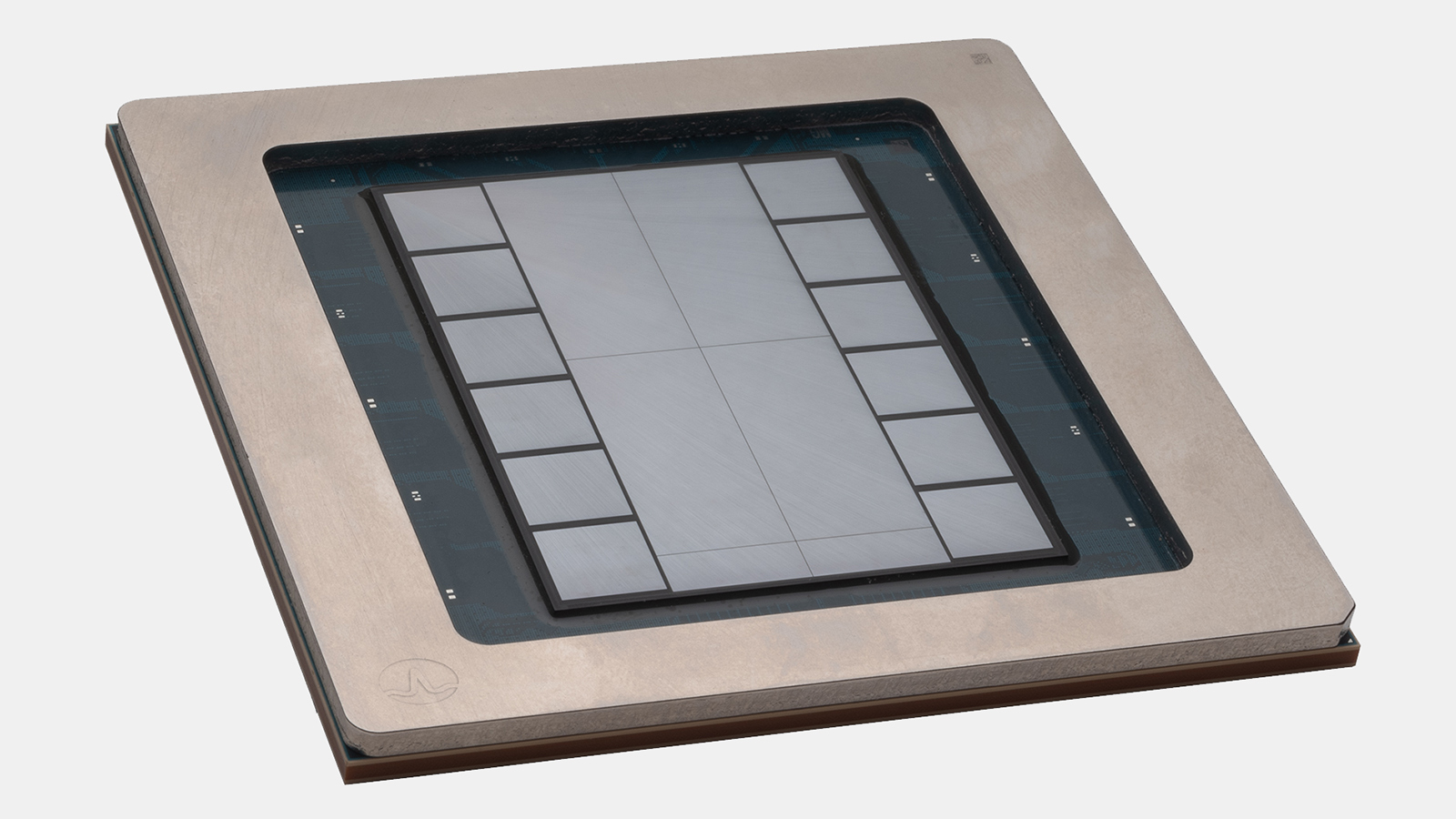
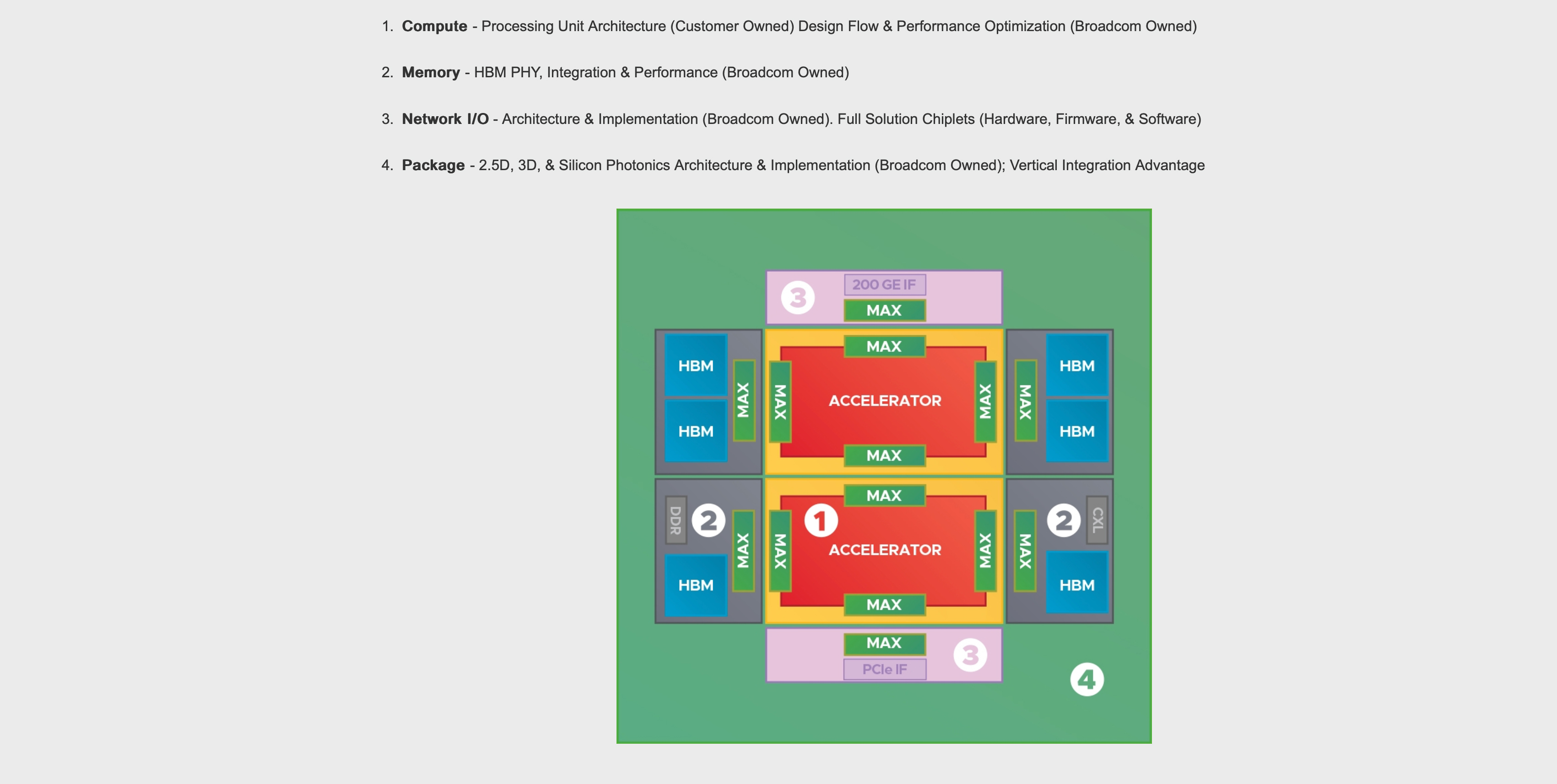
Broadcom has introduced its 3.5D eXtreme Dimension System in Package (3.5D XDSiP) platform for ultra-high-performance processors for AI and HPC workloads. The new platform relies on TSMC's CoWoS and other advanced packaging technologies. It enables chip designers to build system-in-packages (SiPs) of 3D-stacked logic, network and I/O chiplets, and HBM memory stacks. The platform allows for SiPs with up to 6000mm² of 3D-stacked silicon with 12 HBM modules. The first 3.5D XDSiP products are set to arrive in 2026.
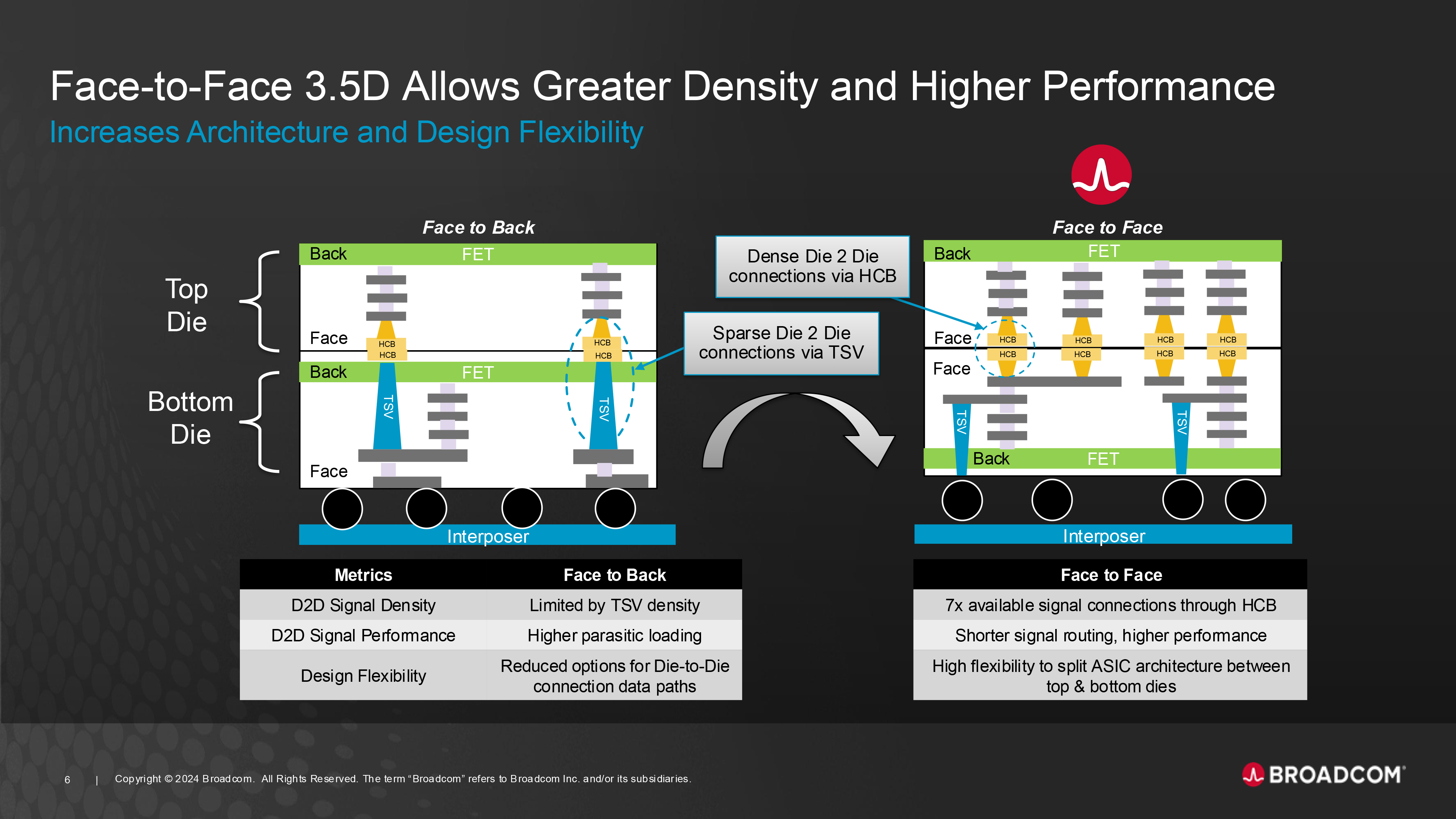
Broadcom's 3.5D XDSiP uses TSMC's CoWoS-L packaging technology that offers a maximum interposer size of approximately 5.5 times that of a reticle (about 858 mm^2), or 4719 mm^2 for compute chiplets, I/O chiplets, and up to 12 HBM3/HBM4 packages. To maximize performance, Broadcom suggests disintegrating the design of compute chiplets and stacking one logic chiplet on top of another in a face-to-face (F2F) manner using hybrid copper bonding (HCB).
This face-to-face (F2F) stacking approach that directly connects the upper metal layers of the top and bottom silicon dies using bumpless hybrid copper bonding is the key benefit of Broadcom's 3D XDSiP platform compared to the face-to-back approach that relies on through silicon vias (TSVs). The F2F approach enables up to 7 times more signal connections and shorter signal routing, reduces power consumption in die-to-die interfaces by 90%, minimizes latency within the 3D stack, and provides additional flexibility for design teams to disaggregate ASIC architecture between top and bottom dies (which is a result of denser connections and lower latencies), according to Broadcom.
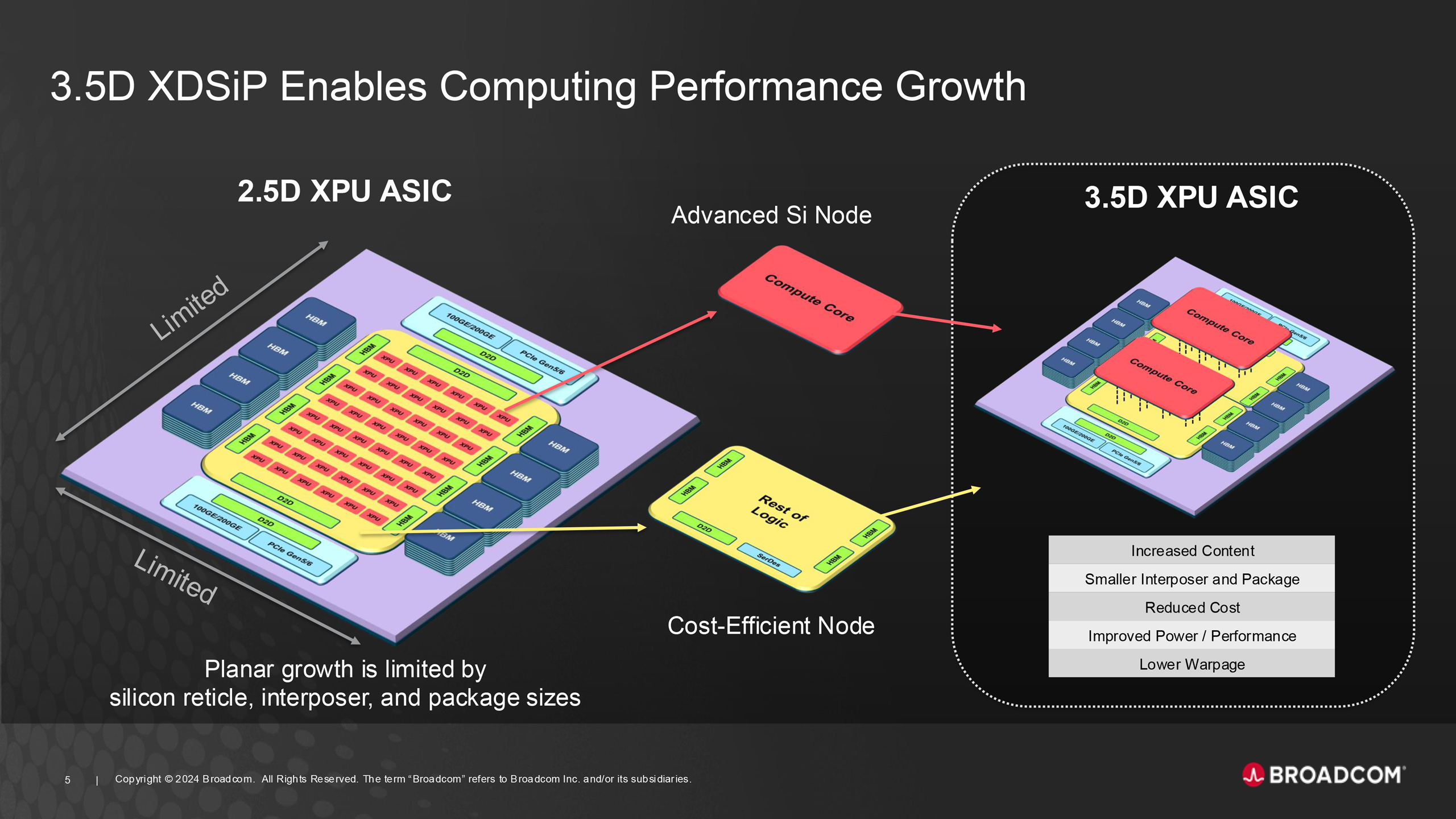
"In close collaboration with our customers, we have created a 3.5D XDSiP platform on top of the technology and tools from TSMC and EDA partners," said Frank Ostojic, Senior Vice President and General Manager, ASIC Products Division, Broadcom. "By stacking chip components vertically, Broadcom's 3.5D platform enables chip designers to pair the right fabrication processes for each component while shrinking the interposer and package size, leading to significant improvements in performance, efficiency, and cost."
The company's press release does not mention TSMC's 3D stacking packaging methods. However, 3.5D XDSiP's F2F HCB is likely a proprietary implementation of TSMC's bumpless SoIC-X stacking technology, albeit with Broadcom's proprietary design and automation flow (which is something indirectly confirmed by Kevin Zhang from TSMC). Since the platform uses both 2.5D integration and 3D stacking, Broadcom calls it '3.5D.'
"TSMC and Broadcom have collaborated closely over the past several years to bring together TSMC's most advanced logic processes and 3D chip stacking technologies with Broadcom's design expertise," said Dr. Kevin Zhang, Senior Vice President of Business Development & Global Sales and Deputy Co-COO, TSMC.
Broadcom is set to use its 3.5D eXtreme Dimension System in Package platform for custom AI/HPC processors and ASICs it designs for companies like Google, Meta, and OpenAI, which have infinite demands for performance. As part of the platform, Broadcom will offer a broad set of IPs, including HBM PHY, PCIe, and GbE; full-solution chiplets; and even silicon photonics, which enables its clients to focus on the essential part of their processors: processing unit architecture.
Stay On the Cutting Edge: Get the Tom's Hardware Newsletter
Get Tom's Hardware's best news and in-depth reviews, straight to your inbox.
Broadcom's lead 3.5D XDSiP product combines four compute dies made on TSMC's leading-edge process technology (N2), one I/O die, and six HBM modules.
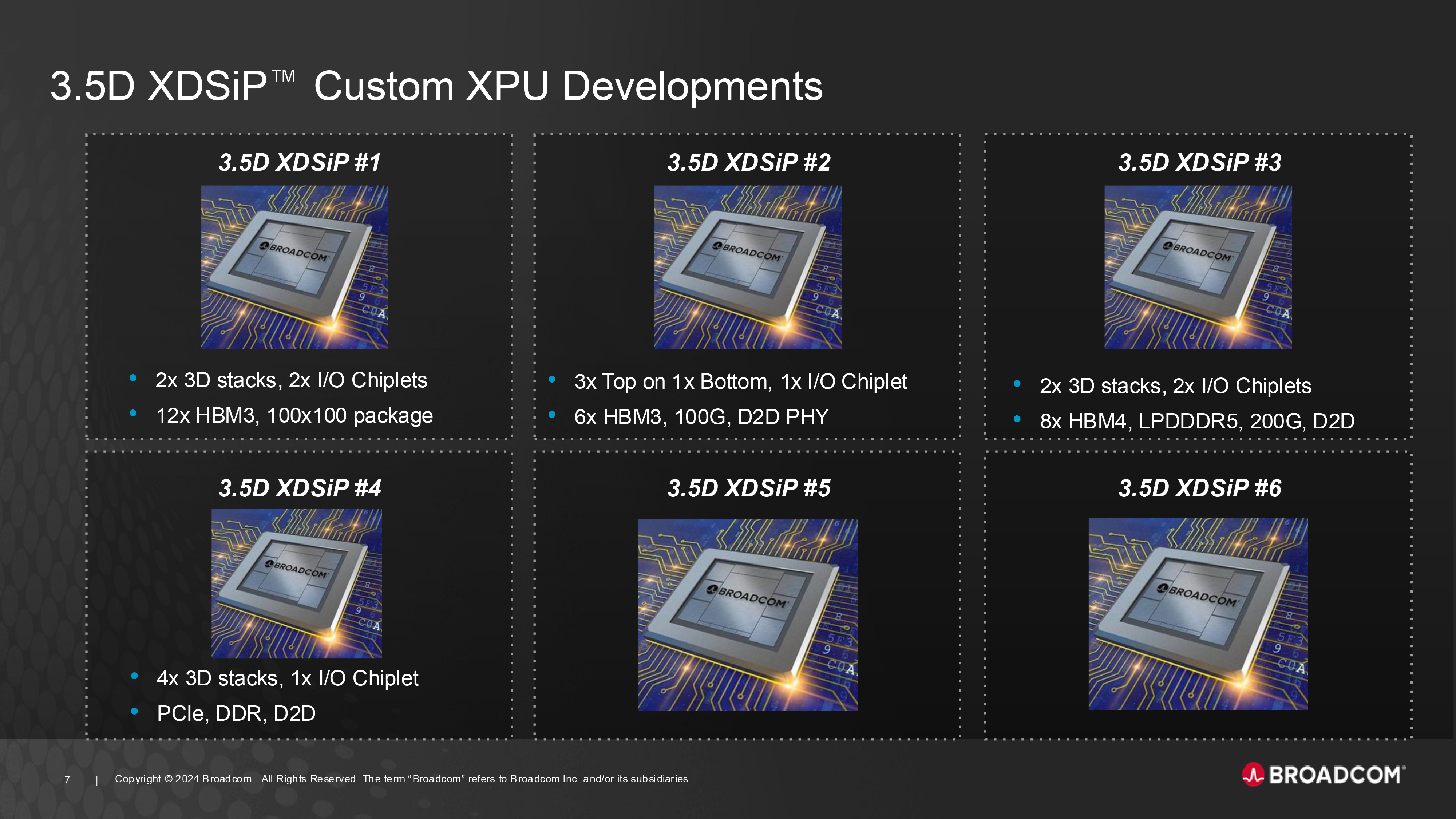
Broadcom currently has five products under development using its 3.5D technology, including several products for the growing AI sector from its major customers and one — the Fujitsu Monaka processor that will use the Arm ISA and TSMC's 2nm-class process technology — aimed at both AI and HPC spaces. Shipments of 3.5D XDSiP products will start in February 2026.
"With over a decade-long partnership, Fujitsu and Broadcom have successfully brought multiple generations of high-performance computing ASICs to the market," said Naoki Shinjo, SVP and Head of Advanced Technology Development at Fujitsu. "Broadcom's latest 3.5D platform enables Fujitsu's next-generation 2-nanometer Arm-based processor, Fujitsu-Monaka, to achieve high performance, low power consumption and lower cost."

Anton Shilov is a contributing writer at Tom’s Hardware. Over the past couple of decades, he has covered everything from CPUs and GPUs to supercomputers and from modern process technologies and latest fab tools to high-tech industry trends.
-
bit_user Didn't AMD use face-to-face stacking for X3D? If the "Cost-Efficient Node" shown in their diagrams is something like TSMC N6, this makes me wonder whether they could also just put the L3 cache in the base tile.Reply