Sohu AI chip claimed to run models 20x faster and cheaper than Nvidia H100 GPUs
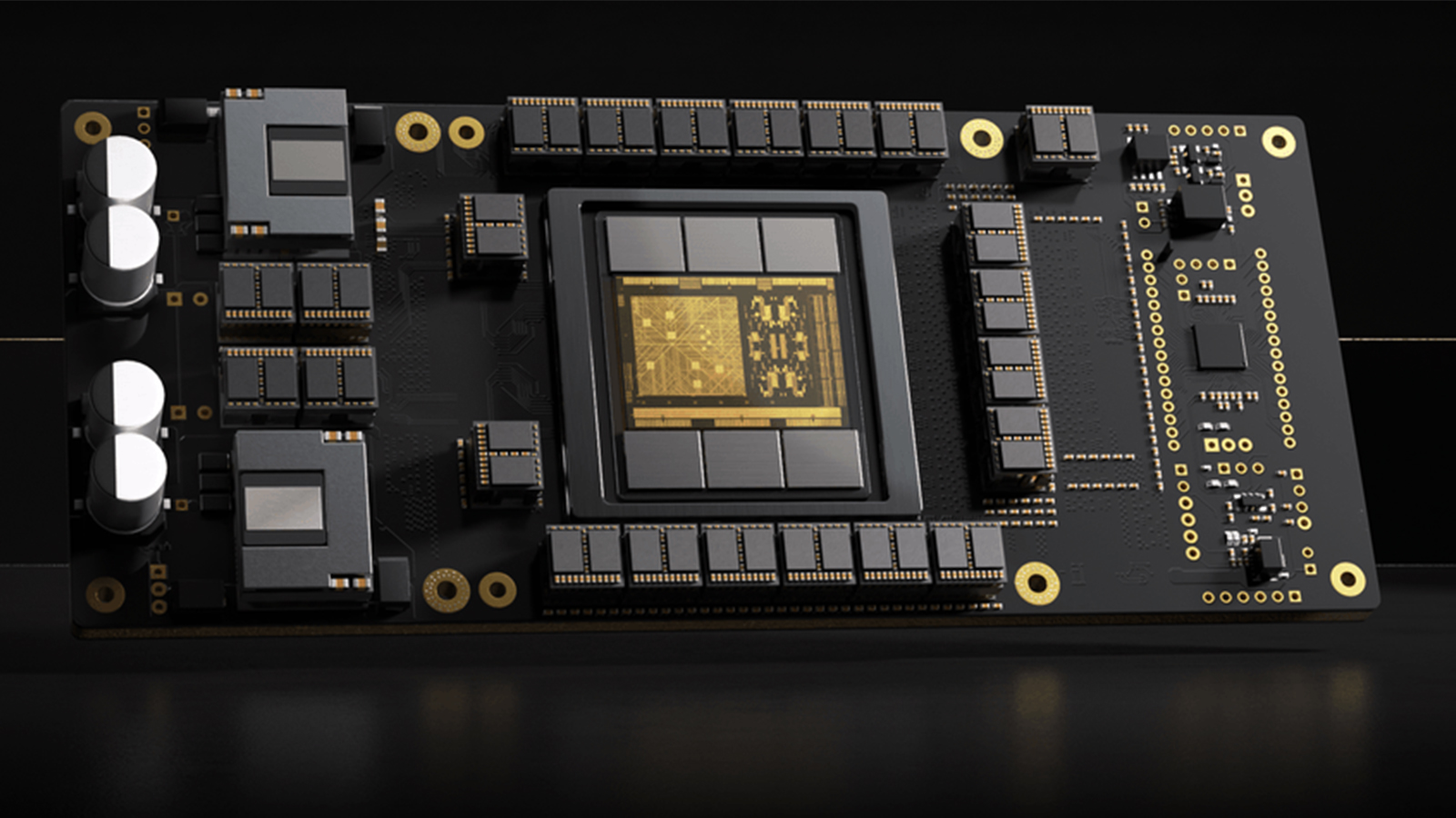
Startup Etched has created this LLM-tuned transformer ASIC.

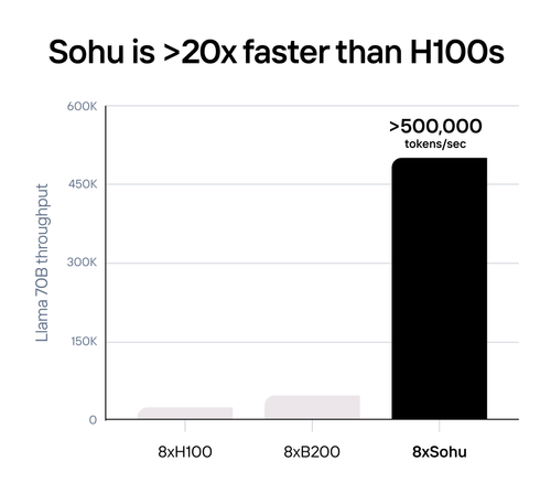
Etched, a startup that builds transformer-focused chips, just announced Sohu, an application-specific integrated circuit (ASIC) that claims to beat Nvidia’s H100 in terms of AI LLM inference. A single 8xSohu server is said to equal the performance of 160 H100 GPUs, meaning data processing centers can save both on initial and operational costs if the Sohu meets expectations.
According to the company, current AI accelerators, whether CPUs or GPUs, are designed to work with different AI architectures. These differing frameworks and designs mean hardware must be able to support various models, like convolution neural networks, long short-term memory networks, state space models, and so on. Because these models are tuned to different architectures, most current AI chips allocate a large portion of their computing power to programmability.
Most large language models (LLMs) use matrix multiplication for the majority of their compute tasks and Etched estimated that Nvidia’s H100 GPUs only use 3.3% percent of their transistors for this key task. This means that the remaining 96.7% silicon is used for other tasks, which are still essential for general-purpose AI chips.
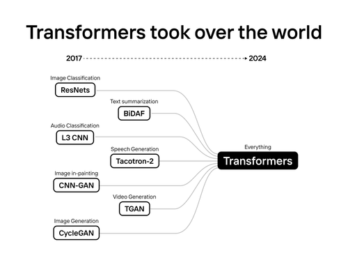
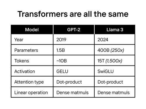
However, the transformer AI architecture has become very popular as of late. For example, ChatGPT, arguably the most popular LLM today, is based on a transformer model. In fact, it’s in the name — Chat generative pre-trained transformer (GPT). Other competing models like Sora, Gemini, Stable Diffusion, and DALL-E are all also based on transformer models.


Etched made a huge bet on transformers a couple of years ago when it started the Sohu project. This chip bakes in the transformer architecture into the hardware, thus allowing it to allocate more transistors to AI compute. We can liken this with processors and graphics cards — let’s say current AI chips are CPUs, which can do many different things, and then the transformer model is like the graphics demands of a game title. Sure, the CPU can still process these graphics demands, but it won’t do it as fast or as efficiently as a GPU. A GPU that’s specialized in processing visuals will make graphics rendering faster and more efficient, that’s because its hardware is specifically designed for that.
This is what Etched did with Sohu. Instead of making a chip that can accommodate every single AI architecture, it built one that only works with transformer models. When it started the project in 2022, ChatGPT didn’t even exist. But then it exploded in popularity in 2023, and the company’s gamble now looks like it is about to pay off — big time.
Nvidia is currently one of the most valuable companies in the world, posting record revenues ever since the demand for AI GPUs surged. It even shipped 3.76M data center GPUs in 2023, and this is trending to grow more this year. But Sohu’s launch could threaten Nvidia’s leadership in the AI space, especially if companies that exclusively use transformer models move to Sohu. After all, efficiency is the key to winning the AI race, and anyone who can run these models on the fastest, most affordable hardware will take the lead.
Get Tom's Hardware's best news and in-depth reviews, straight to your inbox.
Ever since AI data centers started popping up left and right, many experts have raised their concerns over the power consumption crisis this power-hungry infrastructure will lead us to. Meta founder Mark Zuckerberg says electricity supply will constrain AI growth, and even the U.S. government has stepped in to discuss AI power demands. All the GPUs sold last year consume more power than 1.3 million homes, but if Etched’s approach to AI computing with Sohu takes off, we can perhaps reduce AI power demands to more manageable levels, allowing the electricity grid to catch up as our computing needs grow more sustainably.

Jowi Morales is a tech enthusiast with years of experience working in the industry. He’s been writing with several tech publications since 2021, where he’s been interested in tech hardware and consumer electronics.
-
Diogene7 In theory, Intel seems to have shown that their Intel MESO (Magnetoelectric spin-orbit) logic, a post-CMOS technology related to spintronics, is much more amenable to both low-power logic and low-power neuromorphic computing.Reply
For example, emerging Non-Volatile-Memory (NVM) / Persistent Memory MRAM is already based on spintronics phenomena
Therefore much more R&D ressources should be allocated to develop new manufactuting tools to improve and lower MRAM manufacturing cost, and then improve those tools to evolve to MESO manufacturing : this would be much, much more groundbreaking !!!
https://www.techspot.com/news/77688-intel-envisions-meso-logic-devices-superseding-cmos-tech.html
https://www.imec-int.com/en/press/imecs-extremely-scaled-sot-mram-devices-show-record-low-switching-energy-and-virtually -
JTWrenn This was an interesting bit of tech news but....from what I can tell they have yet to actually build a working chip. They just have an idea and not even a fully fleshed out design which they will outsource. Seems like it could be amazing but can anyone find anything saying they have built and tested one? Right now this feels like vaporware with a huge upside if it works but s ton of hurdles to get to there.Reply
Am I wrong on that? Or does this thing only exist on paper right now? -
Diogene7 ReplyJTWrenn said:This was an interesting bit of tech news but....from what I can tell they have yet to actually build a working chip. They just have an idea and not even a fully fleshed out design which they will outsource. Seems like it could be amazing but can anyone find anything saying they have built and tested one? Right now this feels like vaporware with a huge upside if it works but s ton of hurdles to get to there.
Am I wrong on that? Or does this thing only exist on paper right now?
To my knowledge, the European semiconductor research center IMEC was able to build a prototype but not with all needed key metrics.
So indeed there isn’t yet any hard proof yet.
That the reason why I would first allocate significant AI ressources to help find appropriate materials that would help build some prototypes.
From there, more ressources will be needed to build manufacturing tools but some of them may be able to piggy back on MRAM manufacturing tools.
That’s the reason why it is also important to scale up MRAM manufacturing to accelerate the transition to spintronics technology.
My personal belief is that we are currently at the start of the transition from silicon transistors to spintronics, and we are like in the 1950’s / 1960’s when solid state silicon transistors were emerging to replace vacuum tubes… -
CmdrShepard This is so stupid, the time of fixed function hardware was in the 90s. At that time the software technology developed much slower so it made sense to use fixed function hardware to accelerate stuff that wasn't about to change with the next big fad.Reply
Today we have transformers, but tomorrow? And what are datacenters going to do with all those useless ASICs then? More e-waste. At least with H100 you can program and run whatever you want. -
wwenze1 Reply
Crypto ASICs anyoneCmdrShepard said:This is so stupid, the time of fixed function hardware was in the 90s. At that time the software technology developed much slower so it made sense to use fixed function hardware to accelerate stuff that wasn't about to change with the next big fad.
Today we have transformers, but tomorrow? And what are datacenters going to do with all those useless ASICs then? More e-waste. At least with H100 you can program and run whatever you want. -
abufrejoval Reply
Hmm, I can almost picture where you're working (Sophia Antipolis or Grenoble?) or who for (CEA?)Diogene7 said:To my knowledge, the European semiconductor research center IMEC was able to build a prototype but not with all needed key metrics.
So indeed there isn’t yet any hard proof yet.
That the reason why I would first allocate significant AI ressources to help find appropriate materials that would help build some prototypes.
From there, more ressources will be needed to build manufacturing tools but some of them may be able to piggy back on MRAM manufacturing tools.
That’s the reason why it is also important to scale up MRAM manufacturing to accelerate the transition to spintronics technology.
My personal belief is that we are currently at the start of the transition from silicon transistors to spintronics, and we are like in the 1950’s / 1960’s when solid state silicon transistors were emerging to replace vacuum tubes…
I'm afraid you're preaching a reasonable message to the wrong crowd here...
Mais peut-être qu'elle finira par atteindre les personnes qui détiennent la bourse. -
abufrejoval Reply
I'm pretty sure the H100 won't run LibreOffice writer all that well, while I've longed for a GPU-redesigned LibreOffice Calc, basically ever since AMD did demo an HSA variant for Kaveri.CmdrShepard said:This is so stupid, the time of fixed function hardware was in the 90s. At that time the software technology developed much slower so it made sense to use fixed function hardware to accelerate stuff that wasn't about to change with the next big fad.
Today we have transformers, but tomorrow? And what are datacenters going to do with all those useless ASICs then? More e-waste. At least with H100 you can program and run whatever you want.
I've managed to run games on V100s using VirtGL and Steam remote gaming on GPU pass-through VMs, just to prove it can be done.
But I still doubt that recycling H100 or B100 will be much better than trying to squeese value from tons of K40s, P/V100s or in fact anything left over from supercomputers once they've finished their term.
Even at zero purchase cost, the operational expenses kill that older hardware within years and now perhaps months.
Sometimes I'm actually glad I only have kids not shares. -
bit_user Reply
No, a significant chunk of it is used for fp64 and that's definitely not needed for AI!The article said:Most large language models (LLMs) use matrix multiplication for the majority of their compute tasks and Etched estimated that Nvidia’s H100 GPUs only use 3.3% percent of their transistors for this key task. This means that the remaining 96.7% silicon is used for other tasks, which are still essential for general-purpose AI chips.
This is the weird thing: by now, I fully expected Nvidia and AMD to further specialize their high-end silicon on AI and fork the HPC stuff. There's still a chance they might, by the time Etched can ever scale up production of their Sohu chip.
Anyway, this might ultimately be what rains Etched's parade:
https://www.tomshardware.com/tech-industry/artificial-intelligence/ai-researchers-found-a-way-to-run-llms-at-a-lightbulb-esque-13-watts-with-no-loss-in-performance -
bit_user Reply
The V100 is a different animal. It was Nvidia's last to have a full contingent of TMUs and ROPs. The A100 had that stuff on only one SM and I haven't heard of Hopper featuring graphics silicon at all!abufrejoval said:I've managed to run games on V100s using VirtGL and Steam remote gaming on GPU pass-through VMs, just to prove it can be done.
Yeah, for one thing you need a chassis that can host those SXM boards and those won't be cheap, quiet, low-power, or small. And then you've got to pay the electric bill.abufrejoval said:Even at zero purchase cost, the operational expenses kill that older hardware within years and now perhaps months.
Yes, PCIe versions of these GPUs exist, but I'm sure the vast majority of them are of the SXM variety. And the PCIe cards will need a fairly heavy-duty bolt-on cooler, when used outside of a high-airflow server case. -
JTWrenn Reply
I think this is the main point. Nvidia has orders of magnitude more capital and engineers as well as experience in this. The idea that they haven't thought of this approach seems silly.bit_user said:No, a significant chunk of it is used for fp64 and that's definitely not needed for AI!
This is the weird thing: by now, I fully expected Nvidia and AMD to further specialize their high-end silicon on AI and fork the HPC stuff. There's still a chance they might, by the time Etched can ever scale up production of their Sohu chip.
Anyway, this might ultimately be what rains Etched's parade:
https://www.tomshardware.com/tech-industry/artificial-intelligence/ai-researchers-found-a-way-to-run-llms-at-a-lightbulb-esque-13-watts-with-no-loss-in-performance
This is an arms race between companies. At this size with this level of money I don't see Nvidia not going a similar route without a damn good reason. Possibly because they see the fact that AI is still just starting and if you have a custom card for only one type of AI...you could suddenly have a totally obsolete card just by a new AI trend/standard coming out.
