ASE developing square packaging substrate tech to replace round wafers
Organic square substrates?

Get Tom's Hardware's best news and in-depth reviews, straight to your inbox.
You are now subscribed
Your newsletter sign-up was successful
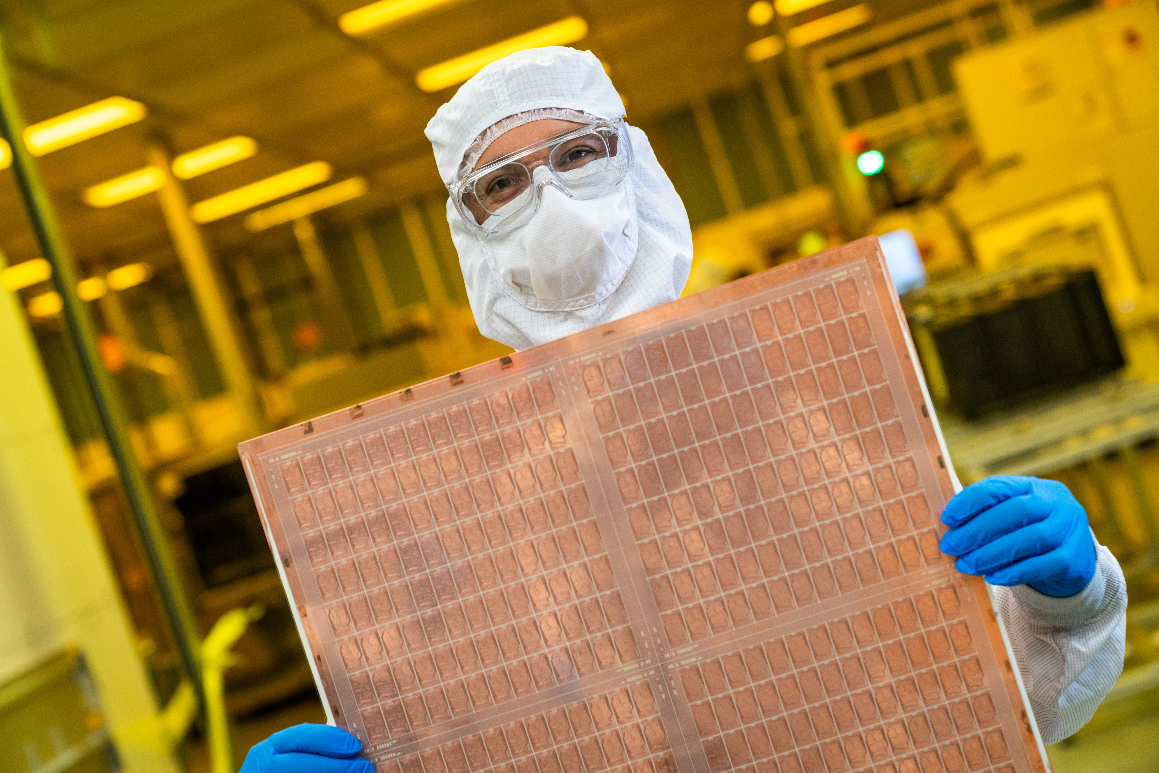
ASE Technology is committing $200 million to test a new method of chip packaging that replaces traditional round wafers with square substrates, which promises to increase the company's advanced packaging output, reports Nikkei. For now, the company plans to set up a rather small-scale trial production line, but the rather large sum that ASE plans to invest indicates that it is serious about using next-gen substrates.
ASE plans to set up a test production line in Kaohsiung, Taiwan, where it would install experimental machines that will process 600mm × 600mm substrates instead of 300-mm round wafers. As no ready-to-use machines can process such large square substrates that meet the requirements of semiconductor-grade production, ASE is collaborating with suppliers to develop the tools to make this technology feasible.
The new 600mm × 600mm substrates could provide up to five times the usable area of 300-mm wafers, allowing more multi-chiplet AI processors to be assembled using one substrate, Tien Wu, chief executive of ASE, explained to reporters. Also, such substrates will enable the company to build bigger multi-chiplet solutions.
Article continues belowIt should be noted that advanced packaging technologies — such as TSMC's CoWoS and similar methods used by ASE or Amkor — rely on tools originally developed for chipmaking. As a result, ASE will have to persuade producers of wafer fabbing equipment to make custom tools for its initiatives. If successful with its square substrates initiative, ASE may leave its rivals behind by several years.
The company will spend $200 million on these new pieces of equipment. However, it is unclear how much the company and its partners will have to pour into research and development of appropriate tools and production methods. For now, ASE hopes to deliver the first customer samples of products assembled on square wafers by next year.
The company’s capital spending for 2025 is expected to surpass the $1.9 billion spent last year, though exact figures have yet to be determined. $200 million will account for around 10% of this sum, which means the square packaging initiative represents a significant investment and serious intentions.
Switching to panel-level packaging could be a precursor to switching to glass substrates (something that Intel, Samsung Foundry, and BOE are looking at) that will not only enable building larger system-in-packages (SiPs) but will improve their flatness, thermal and mechanical stability, as well as enabling denser interconnections.
Get Tom's Hardware's best news and in-depth reviews, straight to your inbox.

Anton Shilov is a contributing writer at Tom’s Hardware. Over the past couple of decades, he has covered everything from CPUs and GPUs to supercomputers and from modern process technologies and latest fab tools to high-tech industry trends.
-
Captnimo This is easier said than done. Most of the Si semiconductor industry had a hell of a time just getting to 300mm, with most of the SiC still struggling to get to 200mm. There’s 450mm, but that’s seen as an Okapi, so rare people don’t even think it exists. Bowing and flatness issues aside, having to respec an entire industry from front to back end would cost hundreds of billions, possibly trillions of dollars - you couldn’t just repurpose old 300mm equipment, since the stage is roughly ~600mm by 600mm; you’d have to build a whole new system for grinders, dicers, probers, lithography, and inspection. Now, not saying it couldn’t be done, however such a leap isn’t going to be easy.Reply