Intel details next-gen 18A fab tech: significantly more performance, lower power, higher density
GAA transistors and backside power delivery seemingly do wonders.

Intel is set to detail (PDF) the advantages of its 18A manufacturing technology (1.8nm-class) compared to its Intel 3 fabrication process at the upcoming VLSI Symposium 2025. As expected, the new production node will offer substantial benefits across power, performance, and area (PPA) metrics, thus providing tangible advantages both for client and data center products.
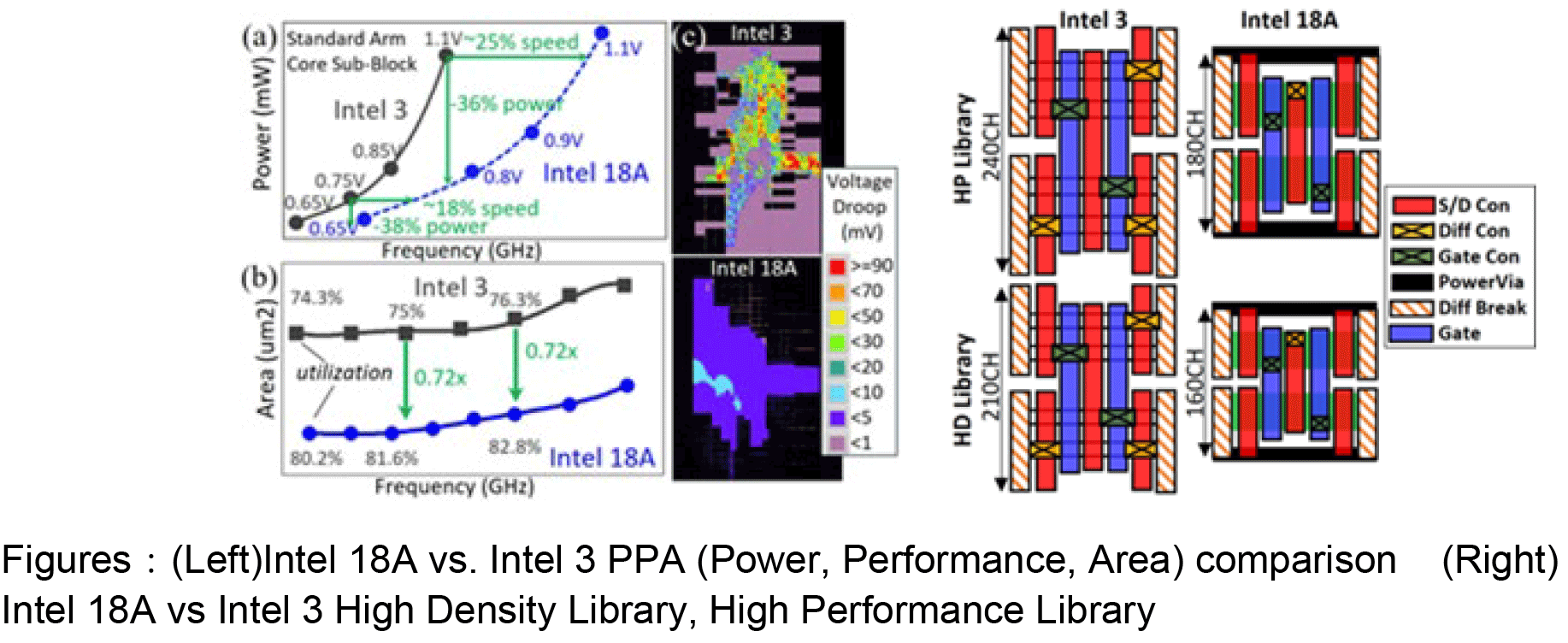
Intel claims that its 18A fabrication process delivers 25% more performance at the same voltage (1.1V) and complexity, as well as 36% lower power at the same frequency and voltage of 1.1V for a standard Arm core sub-block compared to the same block fabricated on Intel 3 process technology. At a lower voltage (0.75V), Intel 18A provides 18% higher performance and 38% lower power. In addition, 18A consistently achieves 0.72X area scaling compared to Intel 3.
Intel's 18A manufacturing technology is the company's first node to rely on gate-all-around (GAA) RibbonFET transistors and feature PowerVia backside power delivery network (BSPDN), two features that enable major PPA advantages.
Article continues belowThe standard cell layout comparison highlights the significant physical scaling achieved by Intel 18A over Intel 3 in both High-Performance (HP) and High-Density (HD) libraries. Intel 18A reduces cell heights from 240CH to 180CH in HP libraries and from 210CH to 160CH in HD libraries, which represents a ~25% reduction in vertical dimension. This tighter cell architecture allows for increased transistor density, contributing directly to improved area efficiency.
The use of PowerVia BSPDN enables more efficient vertical routing by offloading power lines from the front side of ICs, freeing up space for signal routing and further compacting the layout. Additionally, refined gate, source/drain, and contact structures improve overall cell uniformity and integration density. These enhancements collectively enable Intel 18A to deliver better performance-per-area and energy efficiency, supporting more advanced and compact chip designs.
Intel is reportedly on track to start high-volume manufacturing of compute chiplets for its codenamed Panther Lake processors for client PCs later this year and then chiplets for Clearwater Forest data center systems in early 2026. In addition, the company is on track to tape out the first third-party designs on 18A in mid-2025.
Apparently, there is interest in developing third-party chips for Intel 18A. In addition to presenting a general paper describing its 18A technology, Intel plans to present a paper describing a PAM-4 transmitter implemented using 18A production node with a BSPDN that is co-authored by engineers from Intel, Alphawave Semi (a contract chip designer and IP provider), Apple, and Nvidia. This does not necessarily mean that Apple or Nvidia will use Intel's 18A for production silicon, but this at least means that they are interested in checking it out.
Get Tom's Hardware's best news and in-depth reviews, straight to your inbox.
Speaking of Apple and Nvidia, TSMC said that virtually all of its partners plan to adopt its N2 (2nm-class) process technology, so it is reasonable to expect this node to be more widely used than Intel's 18A. Nonetheless, for Intel it is crucial to show that it can develop a competitive node and ramp it to high volume, so 18A will play a vital role for the future of Intel's foundry business.

Anton Shilov is a contributing writer at Tom’s Hardware. Over the past couple of decades, he has covered everything from CPUs and GPUs to supercomputers and from modern process technologies and latest fab tools to high-tech industry trends.
-
bit_user So, how do these gains compare against the predictions and prior information? We always knew 18A would be better than Intel 3, but is Intel on-target?Reply
Another key question, and one we aren't likely to get insight into for a while, is what happens when you remove PowerVia/BSPDN. I believe we previously heard that it adds non-trivial cost, and therefore it's likely some customers will opt to forego it. How competitive is 18A, without it? How do 18A's costs compare to TSMC, with it? -
Kamen Rider Blade Reply
I still think that's TBD infobit_user said:So, how do these gains compare against the predictions and prior information? We always knew 18A would be better than Intel 3, but is Intel on-target?
Another key question, and one we aren't likely to get insight into for a while, is what happens when you remove PowerVia/BSPDN. I believe we previously heard that it adds non-trivial cost, and therefore it's likely some customers will opt to forego it. How competitive is 18A, without it? How do 18A's costs compare to TSMC, with it? -
TheSecondPower Reply
I suspect a limited number of EUV machine deliveries held Intel back from wider production of Intel 4/3. When 18A launches Intel will have had two more years to install EUV machines and even today Intel is avoiding more products on Intel 3, probably to divert resources to 18A. So if yields are comparable it ought to reach a far greater volume than Intel 4 & 3 did.Admin said:Nonetheless, for Intel it is crucial to show that it can develop a competitive node and ramp it to high volume, so 18A will play a vital role for the future of Intel's foundry business. -
thestryker Reply
Intel quietly moved MTL over to Intel 3 with the Core 200 launch and all Intel 3/4 (though I assume they've wound down 4) production is in Ireland. All production at Fab 52 in Arizona will be 18A with Oregon being the other 18A production source. This gives them quite a bit of production flexibility, but I have no doubt they're still paying the price for being so late on EUV.TheSecondPower said:even today Intel is avoiding more products on Intel 3, probably to divert resources to 18A. -
Pigpig still have to see yield rate, if produce 100 wafers but 80 wafers are failed, it is still be considered fail, although that 20 wafers are very powerful.Reply -
JayNor Reply
well, if 80% of the die from a wafer are good, I'm guessing Intel products will start moving to their own fabs.Pigpig said:still have to see yield rate, if produce 100 wafers but 80 wafers are failed, it is still be considered fail, although that 20 wafers are very powerful.
They have already said that their yields are appropriate at this stage in the development ... or, at least PG said that. MJH has given it her vote of approval by scheduling the Panther Lake ramp there, with Clearwater Forest also cleared to go, now that its hybrid bonding issue has been resolved. -
TerryLaze Reply
https://www.techpowerup.com/329613/intel-18a-yields-are-actually-okay-and-the-math-checks-outIt's much less than that, at least for big dies it's assumed to be around 50% ,but that's about the same as TSMC so they seem to be fine.JayNor said:well, if 80% of the die from a wafer are good, I'm guessing Intel products will start moving to their own fabs.
"If we assume that Intel has refined its 18A node more, we can conclude that even with some larger designs hitting the EUV machine reticle limit of 858 mm², Intel's yields could be hitting the 50% mark. If we assume that the best player TSMC achieves a 0.1 defect rate, yields of chips at 858 mm² size are barely above 50% using all available models. That is the fully functioning silicon die, of course" -
jp7189 I'm loving the positive news coming from the 18a development. Hopefully, it's true and not just a hype train for investors.Reply
I do wonder about heat generation with BSPDN. Does it mean greater heat on the back of the chip where it's harder to cool? -
EzzyB I never really doubted this. Intel has had many problems. None of them were ever giving their technical people all of the resources and latest technology they needed to create cutting-edge chips. When management finally made the decision to go all-in and spend $600 million a couple of years ago (more since then) to be the first to get these newest EUV machines from ASML, I considered it a given that it would be a success.Reply
It's still Intel, and they have been producing these chips since they've existed. No one knows more about this than Intel engineers and they haven't forgotten how to make microchips. I think the general public has confused mismanagement with a lack technical prowess. The Intel nerds are as good as anyone. -
bit_user Well, this little party didn't last long.Reply
https://www.tomshardware.com/pc-components/cpus/tsmcs-n2-process-reportedly-lands-orders-from-intel-nova-lake-is-the-likely-application
No matter what the reason, it's certainly not good news. Don't yet know if it's truly a bad sign, but it's never a good sign to move something originally slated for 18A over to TSMC.
