Russia develops its first chipmaking tool — outdated by 30 years from day one
For now, Russia's chipmaking industry is just a few decades behind the industry.

Get Tom's Hardware's best news and in-depth reviews, straight to your inbox.
You are now subscribed
Your newsletter sign-up was successful
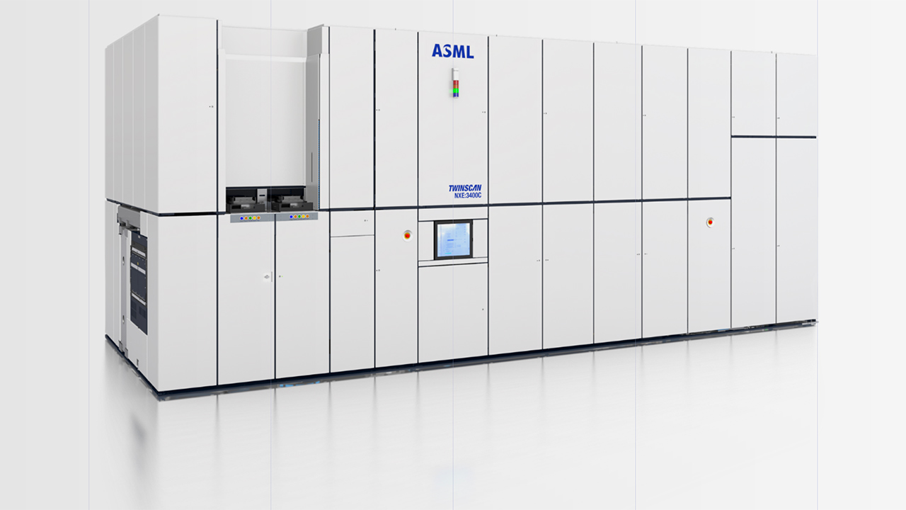
The first Russian photolithography tool, capable of producing chips with a 350 nm process technology or thicker, has been built in Russia and is undergoing testing in Zelenograd. This mature technology is currently used for some automotive and power chips, though it could also be used for military equipment. We estimate that the new piece of equipment is about 30 years behind the industry.
"We assembled and made the first domestic lithographic scanner," Vasily Shpak, Deputy Minister of Industry and Trade of Russia, told TASS. "It is currently undergoing testing as part of the technological line in Zelenograd."
This development marks a significant milestone for Russia's technological capabilities in semiconductor manufacturing. Yet, a 350nm (0.35 micron) is an extremely outdated technology by world-class standards. Intel made its Pentium MMX, Pentium Pro, and initial Pentium II processors on this node in 1995 and 1997, respectively, whereas AMD used this node for its K6 processor in 1997.
Article continues belowEven for Russia, a 350nm fabrication process may be considered outdated as two of the country's contract makers of chips — Angstrem and Mikron — do not offer this production node. Angstrem has a variety of technologies ranging from 250nm to 90nm, whereas Mikron has processes ranging from 250nm to 90nm.
For now, it is unclear how the Russian lithography tool can be used commercially, but we can guess that its main goal is to serve as a development vehicle for more sophisticated litho machines.
Russia's semiconductor sector is developing at a much slower pace than the country's government announced in 2023. Previously stated short-term objectives include ramping up local chip production using 90nm technology by the end of the year, with a long-term goal of establishing 28nm manufacturing by 2027, and then 14nm node by 2030.
An avid reader would ask why Russia needs advanced chipmaking tools if it cannot develop sophisticated chips due to a lack of local talent and the latest electronic design automation tools. It also does not have domestic raw materials to make chips on modern technologies. Furthermore, Russian entities can no longer license advanced CPU cores or chip IP, so they cannot even buy-in the technologies they need to build advanced processors.
Get Tom's Hardware's best news and in-depth reviews, straight to your inbox.

Anton Shilov is a contributing writer at Tom’s Hardware. Over the past couple of decades, he has covered everything from CPUs and GPUs to supercomputers and from modern process technologies and latest fab tools to high-tech industry trends.
-
peachpuff Reply"We assembled and made the first domestic lithographic scanner,"
Found a picture of it...
-
ivan_vy not bad for a country with 1/13th GPD of USA, still too old node to be useful. 350nm is the node Pentium -Pentium II was made.Reply
I think is more like a proof of concept and to training engineers, for everything else they'll have to buy the chinese offerings. -
Eximo As the article states, you can make a lot of useful, and absolutely necessary, electronics with larger nodes. And keep in mind that a lot of military equipment in use today was made well before the Pentium I.Reply -
The Historical Fidelity Reply
Well better late than never I guess. I believe they can manufacture 250nm using multi patterning or even a half node beyond (220nm) with quad patterning. Heck, if SMIC shares their etching technique that allows them to make 5nm class features, perhaps Russia can eke out a 180nm process. It’ll be interesting to see what they can do bringing modern techniques to old lithography technology.ivan_vy said:not bad for a country with 1/13th GPD of USA, still too old node to be useful. 350nm is the node Pentium -Pentium II was made.
I think is more like a proof of concept and to training engineers, for everything else they'll have to buy the chinese offerings. -
blargh4 The world of semiconductors is broader than smartphone SoCs and data center GPUs; there is a heap of silicon in current production that uses 180nm+ lithography. I suspect Russia's priorities lie in beefing up homegrown capabilities for national security related concerns first and foremost, competing with ASML probably isn't too high on that list. They already have domestic production capability for 65nm chips, though clearly not using domestic tools.Reply -
LabRat 891 As I recall, larger lithography chips are much-less liable to be damaged by ionizing radiation, etc.Reply
Kinda reminds me of the post-war technological recovery in the CyberPunk setting.
Anything mid-war and immediately post-war, was 'primitive' on purpose.