Russia to spend $2.54 billion on its own chipmaking tools industry by 2030
A new vague plan pins domestic 65nm to 2030.

Russia has allocated over 240 billion rubles ($2.54 billion) to support a large-scale program to replace foreign chipmaking equipment by 2030, reports CNews.
The initiative involves launching 110 research and development (R&D) projects to reduce dependence on imported wafer fab tools and eventually make chips on a 28nm-class process technology. To put the $2.54 billion number into context, that is 57 times less than the country will spend on defense in its war against Ukraine in 2025 alone.
A broad program to localize chipmaking
Russian chipmakers — Angstrem, Mikron, etc. — can produce chips on various mature nodes, including 65nm and 90nm. Of the 400 tools used in Russia for chips, only 12% can currently be manufactured locally. Sanctions have further complicated the situation, driving up the cost of crucial equipment by 40% – 50% as it must be smuggled to the country. To mitigate costs and reduce reliance on foreign tools, Russia's Ministry of Industry (Minpromtorg) and Trade and MIET (a government-controlled company) have developed a program with a focus on developing domestic alternatives for approximately 70% of the equipment and raw materials required in microelectronics production.
The program covers various aspects of chipmaking, including actual tools, raw materials, and electronic design automation (EDA) tools. The project will develop '20 different technology routes,' such as microelectronics ranging from 180nm to 28nm, microwave electronics, photonics, and power electronics. Some developed technology will also be used for photomask production and electronic module assembly.
With very vague goals
While the program's strategic goals look clear (localize 70% of chipmaking tools and raw materials by 2030 for $2.54 billion), the details look rather vague, to put it mildly.
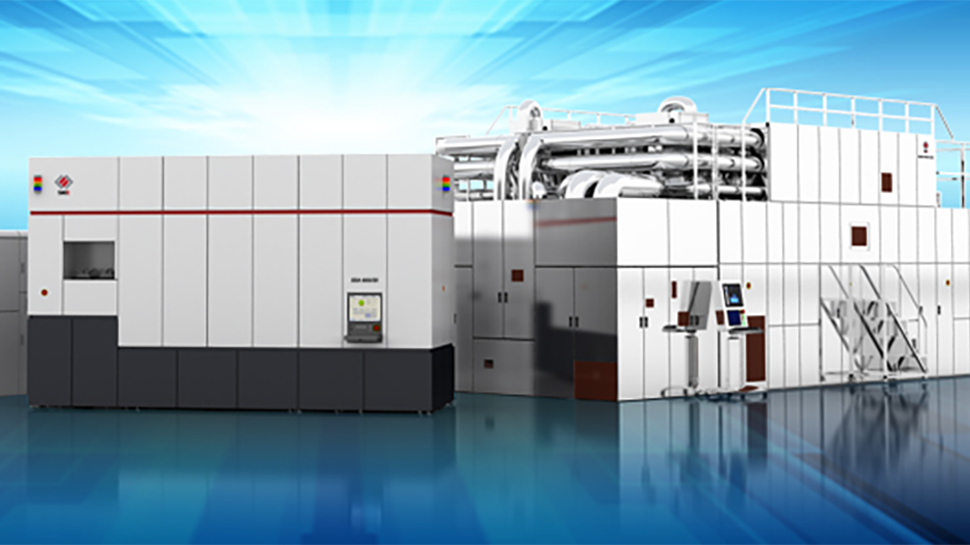
One of the significant milestones expected by the end of 2026 is to develop lithography equipment for 350nm and 130nm process technologies (a massive difference because there are several nodes between 350nm and 130nm nodes) and electron-beam lithography equipment for 150nm production nodes. In addition, the country plans to develop its epitaxy by chemical vapor deposition equipment in a couple of years. Also, by the end of 2026, Russia's Minpromtorg wants the domestic semiconductor industry to produce silicon ingots and cut them into wafers.
By 2030, Russia aims to produce domestic lithography systems capable of processing wafers with 65nm or 90nm process technologies. This would significantly advance the country's ability to produce microelectronics, but it would still be 25 - 28 years behind the industry.
Get Tom's Hardware's best news and in-depth reviews, straight to your inbox.
This new plan certainly looks less ambitious than the one published a year ago, which pinned 28nm to 2027 and the 14nm manufacturing process to 2030 (which can be explained by the fact that last year, the Russian government thought that it could get sophisticated fab tools from global leaders). Yet, it is ambitious enough from the number of tools that are planned to be developed (there is no word about mass production) in the coming years.
The program envisions developing various equipment types, including 15 kinds of control and measurement devices, 13 types of plasma chemical installations, ten types of lithography systems, nine types of tools for chip packaging, eight to make photomasks, seven for wafer production, and so on.

Anton Shilov is a contributing writer at Tom’s Hardware. Over the past couple of decades, he has covered everything from CPUs and GPUs to supercomputers and from modern process technologies and latest fab tools to high-tech industry trends.
-
jkflipflop98 Don't get me wrong, $2.5B is A LOT of money. But that being said, in the semiconductor industry it's chicken scratch. $2.5B wouldn't even pay for the construction of a leading-edge factory shell. It wouldn't come close to purchasing the tools you need to startup a fab. And it's nowhere in the ballpark of funding hail-mary moonshot attempts at leapfrogging the established players in the industry.Reply -
dalek1234 Let me fix the first sentence for you:Reply
"Russia has allocated over 240 billion rubles ($2.54 billion) to support a large-scale program to replace foreign chipmaking equipment by 2030, reports CNews. embezzlement by officials. None of the funds will be spent on chip making "
....but this one is probably more realistic:
"Russia has allocated nothing, but wants others to believe the opposite" -
das_stig Time for all the chip plants to lock their doors for the Russki spies are coming, then again, they'll probably just ask the Chinese spies who have already paid a visit and got the blueprints. :unsure:Reply -
AkroZ Reply
It's precised that this plan doesn't mention mass production, this is just fonds to research the process.jkflipflop98 said:Don't get me wrong, $2.5B is A LOT of money. But that being said, in the semiconductor industry it's chicken scratch. $2.5B wouldn't even pay for the construction of a leading-edge factory shell. It wouldn't come close to purchasing the tools you need to startup a fab. And it's nowhere in the ballpark of funding hail-mary moonshot attempts at leapfrogging the established players in the industry.