
Intel might axe the 18A process node for foundry customers, essentially leaving TSMC with no rival — Intel reportedly to focus on 14A (Updated)
TSMC's N2 and A16 may have no rivals

Lip-Bu Tan, the chief executive of Intel, is considering stopping the promotion of the company's 18A fabrication technology (1.8nm-class) to foundry customers, instead shifting the company's efforts to its next-generation 14A manufacturing process (1.4nm-class) in a bid to secure orders from large customers like Apple or Nvidia, reports Reuters. If this shift in focus occurs, it would be the second node in a row that Intel has deprioritized.
The proposed adjustment could result in major financial consequences and alter the trajectory of Intel's foundry operations, as it will effectively withdraw the company from the foundry market for several years. Intel informs us that the information is based on market speculation. However, the spokesperson provided some additional insight on the company's roadmap, which we've added further below.
“We are not going to comment on market rumors and speculation," an Intel spokesperson said to Tom's Hardware. "As we have said previously, we are committed to strengthening our roadmap, delivering for our customers and improving our financial position for the future."
Lip-Bu Tan proposes killing 18A as a foundry node
After taking the helm in March, Lip-Bu Tan announced intentions to cut costs in April, which is expected to involve layoffs and the cancellation of certain projects. According to the new report, by June, he began sharing with colleagues that the 18A manufacturing process — a technology designed to showcase Intel's manufacturing prowess — was losing appeal to outside customers, which is why he believed it made sense for the company to shift away from offering 18A and its performance-enhanced 18A-P version to foundry customers.
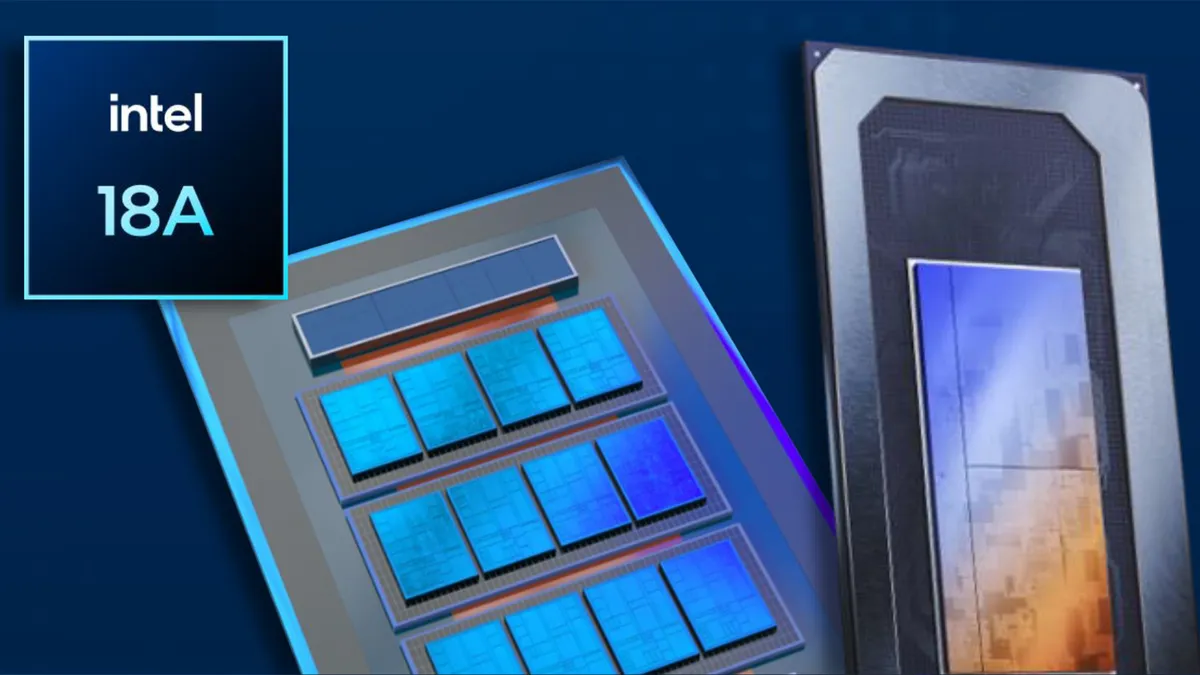
Instead, Lip-Bu Tan proposed directing more resources to the completion and promotion of 14A, the company's next-generation node, which will be ready for risk production in 2027 and for volume production in 2028. Given the timing of 14A, it is now time to start promoting it among potential third-party Intel Foundry clients.
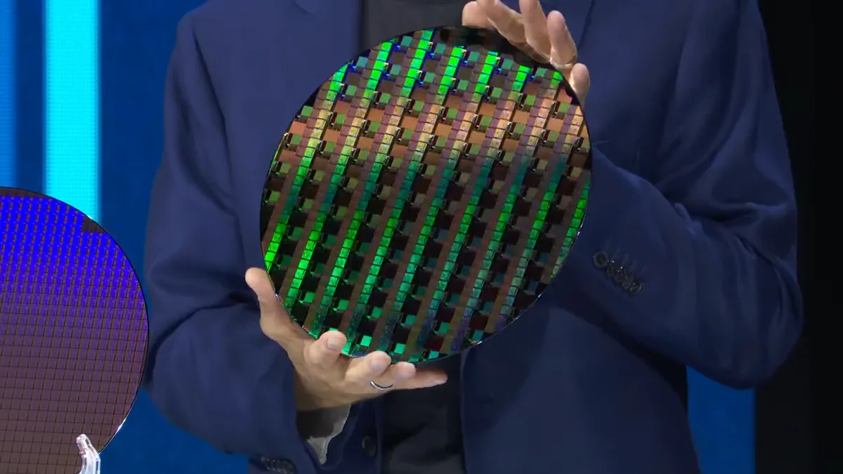
Intel's 18A fabrication technology is the company's first node to utilize its 2nd-generation RibbonFET gate-all-around (GAA) transistors, along with a PowerVia backside power delivery network (BSPDN).
By contrast, 14A utilizes RibbonFET 2 transistors, PowerDirect BSPDN, which delivers power directly to each transistor's source and drain through specialized contacts, and features Turbo Cells for critical paths. In addition, 18A is Intel's first leading-edge technology that is compatible with third-party design tools and can be used by its foundry customers.
Massive write offs vs. depreciation costs
Dropping external sales of 18A and 18A-P would require Intel to account for a substantial write-off reflecting the billions it spent developing the manufacturing technologies, according to individuals familiar with internal deliberations cited by Reuters. Depending on how you count development costs, the resulting charge could total hundreds of millions or even billions of dollars.
Both RibbonFET and PowerVia were initially developed for 20A, but that technology was cancelled for internal products last August in a bid to focus on 18A for both internal and external products.

Intel's rationale behind the move may be rather simple. By limiting the number of potential customers for 18A, the company may potentially cut its operating costs. The majority of tools required for 20A, 18A, and 14A (except for High-NA EUV equipment) are already in place at its Fab D1D in Oregon, as well as at Fabs 52 and 62 in Arizona. However, once these tools are formally put into operation, the company will have to report their depreciation as a cost. Not putting them online potentially enables Intel to cut its costs amid uncertainties with orders from third-party clients.
In addition, by not offering 18A and 18A-P to external customers, Intel may save money on engineers dedicated to supporting the sampling, ramp, and mass production of third-party circuits at Intel fabs. Obviously, this is speculation on our side.
However, by ceasing to offer 18A and 18A-P to external clients, Intel will be unable to demonstrate advantages of its fabrication nodes to a broad range of customers with various designs, which would leave them with a single choice for next two or three years: go with TSMC and use N2, N2P, or even A16.
Although Samsung is set to formally start making chips on its SF2 (also known as SF3P) node later this year, that node is expected to be behind Intel 18A and TSMC's N2 and A16 in terms of power, performance, and area.
Essentially, Intel would not be showing up to its fight against TSMC's N2 and A16, which will certainly not help to gain the confidence of potential clients towards other Intel offerings, namely 14A, 3-T/3-E, Intel/UMC 12nm, and others.
Reuters' sources familiar with the matter explained that Lip-Bu Tan had asked Intel's specialists to prepare proposals for discussion with Intel's board this fall. Options could include ceasing efforts to sign up new clients for 18A, though given the scale and complexity of the issue, the decision might not be finalized until the board meets again later this year.
Intel itself reportedly declined to discuss hypothetical scenarios but confirmed that the main customer for 18A has always been its own Products division, which plans to begin producing codenamed Panther Lake CPUs for laptops in 2025 using this technology. Eventually, 18A and 18A-P will be adopted by Clearwater Forest, Diamond Rapids, and Jaguar Shores products.
Limited demand?
Intel's push to attract large-scale external clients to its Intel Foundry fabs remains critical to its turnaround, as only with high volumes the company will be able to pay off for its process technologies that cost billions to develop.
However, in addition to Intel itself, only Amazon, Microsoft, and the U.S. Department of Defence have formally confirmed plans to use 18A. While Broadcom and Nvidia are also reportedly testing Intel's latest process technology, they have yet to commit to using it for actual products.
Intel's 18A has one key advantage over TSMC's N2: it features backside power delivery, which is particularly useful for power-hungry processors aimed at AI and HPC applications. TSMC's A16 with Super Power Rail (SPR) will only enter mass production in late 2026, so 18A will maintain the advantage of offering backside power delivery for Amazon, Microsoft, and potentially other customers for a while.
However, N2 is expected to offer higher transistor density, which is beneficial for the vast majority of chip designs. Furthermore, while Intel has been running Panther Lake silicon at its D1D fab for quarters (so, currently Intel is still in risk production using 18A), the company's high-volume Fab 52 and Fab 62 started to run 18A test silicon this March, so they will start producing commercial chips only late in 2025, or rather in early 2025.
Intel's external customers are, of course, interested in producing their designs at high-volume fabs in Arizona rather than at development fabs in Oregon.
Summary
Intel CEO Lip-Bu Tan is reportedly considering halting the promotion of the company's 18A fabrication process to external clients and instead focusing on the next-generation 14A production node, aiming to attract large customers such as Apple and Nvidia.
The move could trigger massive write-offs, as Intel has spent billions developing 18A and 18A-P process technologies. Shifting focus to 14A could help cut costs and better prepare the node and operations for third-party clients, but the move risks undermining customer confidence in Intel's foundry capabilities ahead of 14A's planned production in 2027–2028.
While the 18A node remains critical for Intel’s own products, such as Panther Lake CPUs, limited demand from third parties — so far, only Amazon, Microsoft, and the U.S. Department of Defense have confirmed plans to use it — has raised concerns about its viability.
The potential decision — which will essentially withdraw Intel from the broad foundry market until 14A comes to market — will be reviewed by Intel's board later this year. Even if Intel eventually chooses to remove 18A from its foundry offerings, aimed at a broad range of applications and clients, the company will still manufacture chips using 18A for its own products, which are already designed for the process. It also intends to fulfill limited orders it has already committed to, including supplying chips for the aforementioned clients.
Follow Tom's Hardware on Google News to get our up-to-date news, analysis, and reviews in your feeds. Make sure to click the Follow button.

Anton Shilov is a contributing writer at Tom’s Hardware. Over the past couple of decades, he has covered everything from CPUs and GPUs to supercomputers and from modern process technologies and latest fab tools to high-tech industry trends.
-
User of Computers Intel has been saying since Foundry Direct Connect that 18A is a mostly internal node, and that 18A-P is what customers were more interested in. This isn't really news?Reply -
DHB Reply
Instead of writing 18a off why not charge what Apple can’t refuse? Or for loss not to excede write off/loss? And get a customer in the process.User of Computers said:Intel has been saying since Foundry Direct Connect that 18A is a mostly internal node, and that 18A-P is what customers were more interested in. This isn't really news?
I don’t get the company’s thinking and as my background is software, so just my naive 2¢.
Paying the cost to develop for a new process may not make sense if 18a isn’t sufficiently better than TSMC, but getting another supplier usually is a good thing. (However, If it ain’t broke…) -
sseemaku Just saw a post few days back that demand for advanced nodes has skyrocketed. And then we have Intel struggling to get any customers for its advanced node. I hope people more knowledgeable can throw some light on what are the issues with 18A.Reply -
TerryLaze Reply
What do you mean by "writing off" ? They are going to use 18A the same way they used all of their nodes from since they became intel, they will make a full line up and sell them.DHB said:Instead of writing 18a off why not charge what Apple can’t refuse? Or equivalent to write off loss?
With only two foundries that make 18A there is probably no space for anybody else's products anyway.
Intel will have to get a few more fabs running for them to have enough fabs to produce for others as well. -
JamesJones44 Presumably Intel is still using 18A internally for their own up coming processors. Some of that would not be allowed to be written off. Intel would have to show without a doubt that the machines are being "scrapped" and not used for other purpose. It could save money by not scaling a node to other fabs due to low external demand, but I'm a little more skeptical about how much they will actually be able to write down if they still use the nodes for internal products. I suppose if they only produce their internal products at one site, they could write off/down the others.Reply -
Eximo Reply
Not if it gets used by Intel. They did skip 20A I suppose. If they use all the manufacturing capacity to make Core and Xeon, and maybe Arc tiles/GPUs I would call that a success. Even if Intel doesn't end up competing well.S58_is_the_goat said:Is this the new 10nm? -
TerryLaze ReplyJamesJones44 said:Presumably Intel is still using 18A internally for their own up coming processors. Some of that would not be allowed to be written off. Intel would have to show without a doubt that the machines are being "scrapped" and not used for other purpose. It could save money by not scaling a node to other fabs due to low external demand, but I'm a little more skeptical about how much they will actually be able to write down if they still use the nodes for internal products. I suppose if they only produce their internal products at one site, they could write off/down the others.However, in addition to Intel itself, only Amazon, Microsoft, and the U.S. Department of Defence have formally confirmed plans to use 18A. While Broadcom and Nvidia are also reportedly testing Intel's latest process technology, they have yet to commit to using it for actual products.
Ms=15B
US DoD=3B
Amazon= "multibillion"
Intel itself= ~17B gross last year and that was using tsmc, so that would be a minimum for their own node.
That should cover the expenses of the 2 or three FABs that are ready to make 18A, they spend about 90B until now so they will be getting back a good chunk of that.