Chinese university builds 3D chip design tool tailored to Huawei's ‘LogicFolding’ architecture — 3D design delivers increased performance and better thermal management

huawei company floor
(Image credit: Getty Images)

Peking University's School of Integrated Circuits has unveiled a prototype electronic design automation (EDA) tool built specifically for Huawei's LogicFolding architecture, according to the South China Morning Post. The tool takes what researchers described as a "true-3D" approach, optimizing an entire multilayer chip as a single vertical structure rather than designing each layer in two dimensions and stacking them afterward. In early tests of open-source circuit designs, the university reported a 30% reduction in total internal wire length, along with improvements in performance and thermal management, compared to conventional EDA workflows.

The announcement came two days after Huawei presented LogicFolding and its accompanying Tau Scaling Law at the IEEE International Symposium on Circuits and Systems (ISCAS 2026) in Shanghai. Huawei's goal is to produce chips with transistor density equivalent to 1.4nm processes by 2031, all without access to the extreme ultraviolet (EUV) lithography equipment restricted under U.S. export controls.

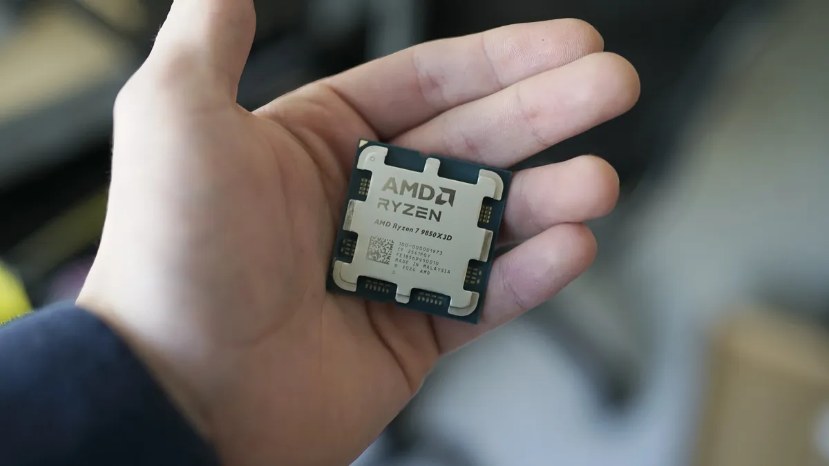
LogicFolding works by folding traditional 2D circuit layouts into vertical 3D stacks, shortening the physical paths that electrical signals travel through a chip. That reduces resistance and capacitance on critical wiring, compressing signal propagation delay. Huawei's Kirin smartphone processors launching later this year will be the first commercial chips to use the architecture.

Latest Videos From

Synopsys and Cadence both offer 3D IC design platforms for multi-die stacking and advanced packaging. But those tools address a different problem: integrating separate chiplets or dies within a package. LogicFolding folds transistor-level logic within a single chip into vertical layers, an intra-die optimization that requires place-and-route tools to work across the full vertical structure simultaneously instead of partitioning separate dies.

Peking University's prototype reportedly addresses this by treating the multilayer structure as a unified design space from the start, but whether their claim of 30% wire-length improvement holds up at production scale remains to be seen.

Synopsys, Cadence, and Siemens EDA command 31%, 30%, and 13% of the global EDA market, respectively, and their combined share within China exceeds 80%, according to EE Times China. The U.S. imposed and then lifted EDA export restrictions last year as part of a rare-earth materials deal. Still, the episode highlighted how dependent Chinese chipmakers remain on Western tools.

China's domestic EDA companies, including Empyrean Technology and Primarius, have made progress in analog, mixed-signal, and physical verification, but none offer a full digital design flow competitive with the Western incumbents at advanced nodes.

A university prototype is a very long way from production-grade commercial software. EDA tools require years of development, extensive process design kit integration with foundries, and validation across thousands of tape-outs before chipmakers trust them. "No single company can independently find all the answers along the path of semiconductor evolution," He Tingbo, chairwoman of the Huawei Scientist Committee and president of the company's semiconductor business department, said at a media briefing on Monday.

Google Preferred Source

Follow Tom's Hardware on Google News, or add us as a preferred source, to get our latest news, analysis, & reviews in your feeds.

TOPICS
Luke James
Contributor

Luke James is a freelance writer and journalist.  Although his background is in legal, he has a personal interest in all things tech, especially hardware and microelectronics, and anything regulatory. 

  • urn66
    The importance of this should not be underestimated. Beyond the obvious improvements of concurrent design on multiple layers and the related benefits designing IC and package in one stack (something conventional 2D EDA tools do ins sequential interactions) is the strategic importance of this is to liberate Chinese designers who have suffered US embargoes of high-level design tools under Biden and Trump. The fact that a full-stack package is released concurrently wth the Huawei announcement shows a level of cooperation that will be critical to the success of the method. So once again, thanks to Biden and Trump for Making China Great Again.
    Reply
  • A_XTX24G
    Hmm, sounds great but application matters, for most, a phone is a phone.
    Reply
  • Conor Stewart
    A_XTX24G said:
    Hmm, sounds great but application matters, for most, a phone is a phone.
    That is just the first application of it. Why would it be limited to phones? We will likely see more and more chips being built with it.
    Reply
  • A_XTX24G
    Conor Stewart said:
    That is just the first application of it. Why would it be limited to phones? We will likely see more and more chips being built with it.
    On the question, sure why not?
    On the rest, pure speculation with no grounded root.

    There are many examples of technically impressive chip technologies that never achieved widespread adoption because of:


    Cost
    Manufacturing complexity
    Yield issues
    Packaging challenges
    Software/ecosystem limitations
    Competition from alternative approaches
    Intel Optane / 3D XPointPromised a revolutionary middle ground between DRAM and NAND flash.
    Technically impressive with low latency and high endurance.
    Never achieved broad adoption due to cost, ecosystem inertia, and limited use cases.Intel ItaniumIntended to replace x86 in high-performance computing.
    Massive engineering effort and significant technical innovation.
    Ultimately failed because x86 evolved faster and software compatibility mattered more.Intel EMIB and Foveros (early years)Advanced packaging technologies that generated enormous excitement.
    Adoption has been much slower and more selective than initial marketing implied because of cost and manufacturing complexity.IBM Cell ProcessorExtremely powerful and innovative architecture used in the PlayStation 3.
    Programming complexity limited broader industry adoption.HBM for consumer GPUsTechnically superior in several respects to GDDR memory.
    Appeared in products such as the Radeon R9 Fury X.
    Cost and packaging complexity restricted widespread deployment for years.Monolithic 3D IC researchResearchers have been demonstrating various forms of vertical transistor stacking and 3D logic integration for decades.
    Many promising papers and prototypes exist.
    Commercial deployment has been far slower than the technical promise suggested.
    3D chip designs themselves are not new. Technologies like 3D stacking have existed for years, yet adoption has been selective because the trade-offs are significant.

    Maybe this architecture becomes widely adopted, maybe it doesn't. Nothing in the article establishes that "we will likely see more and more chips built with it."
    Reply