Quantum diamond scanner delivers non-invasive 3D imaging of semiconductors — EuQlid Qu-MRI could ‘save chip foundries billions of dollars’
Company has emerged from stealth with a very healthy order book.

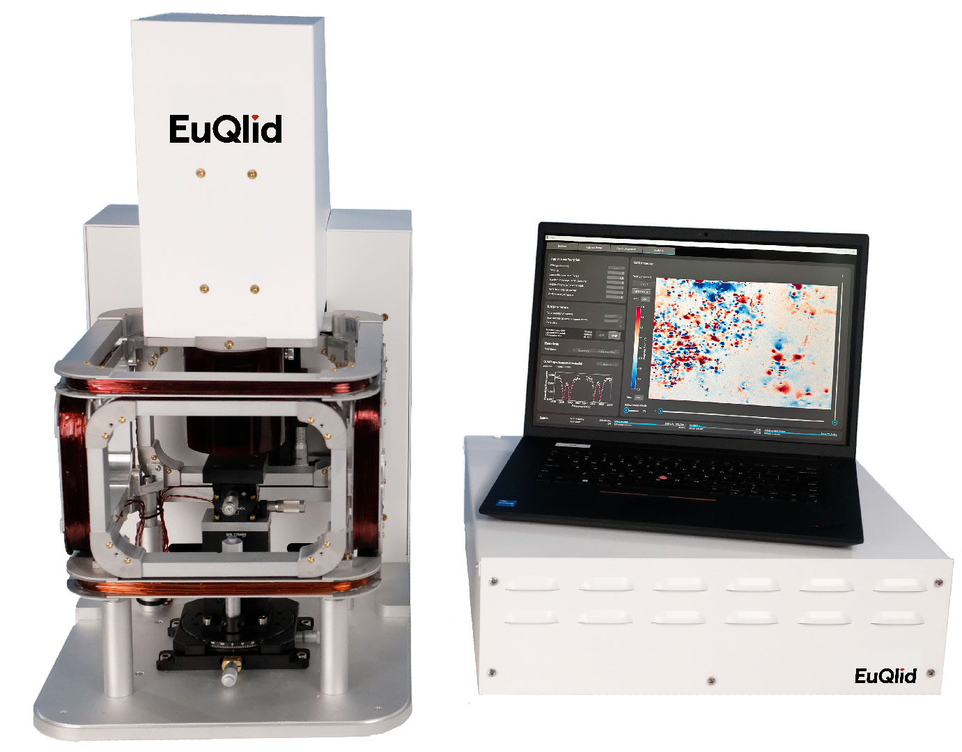
A startup founded by an array of experts from Harvard, Yale, University of Maryland, Cadence, and Texas Instruments has come out of stealth to present a breakthrough device for the non-invasive, non-destructive 3D imaging of semiconductors and batteries.
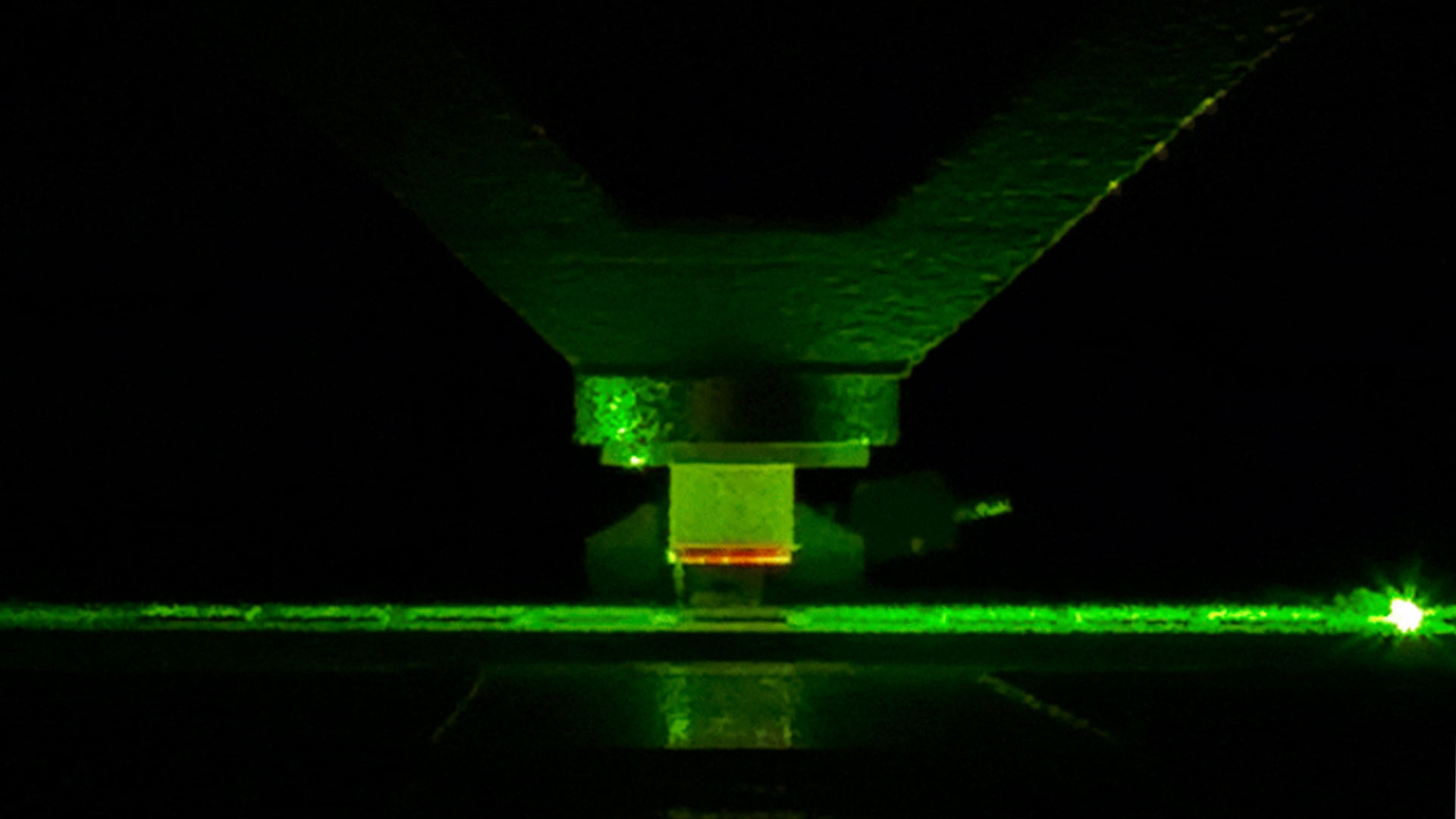
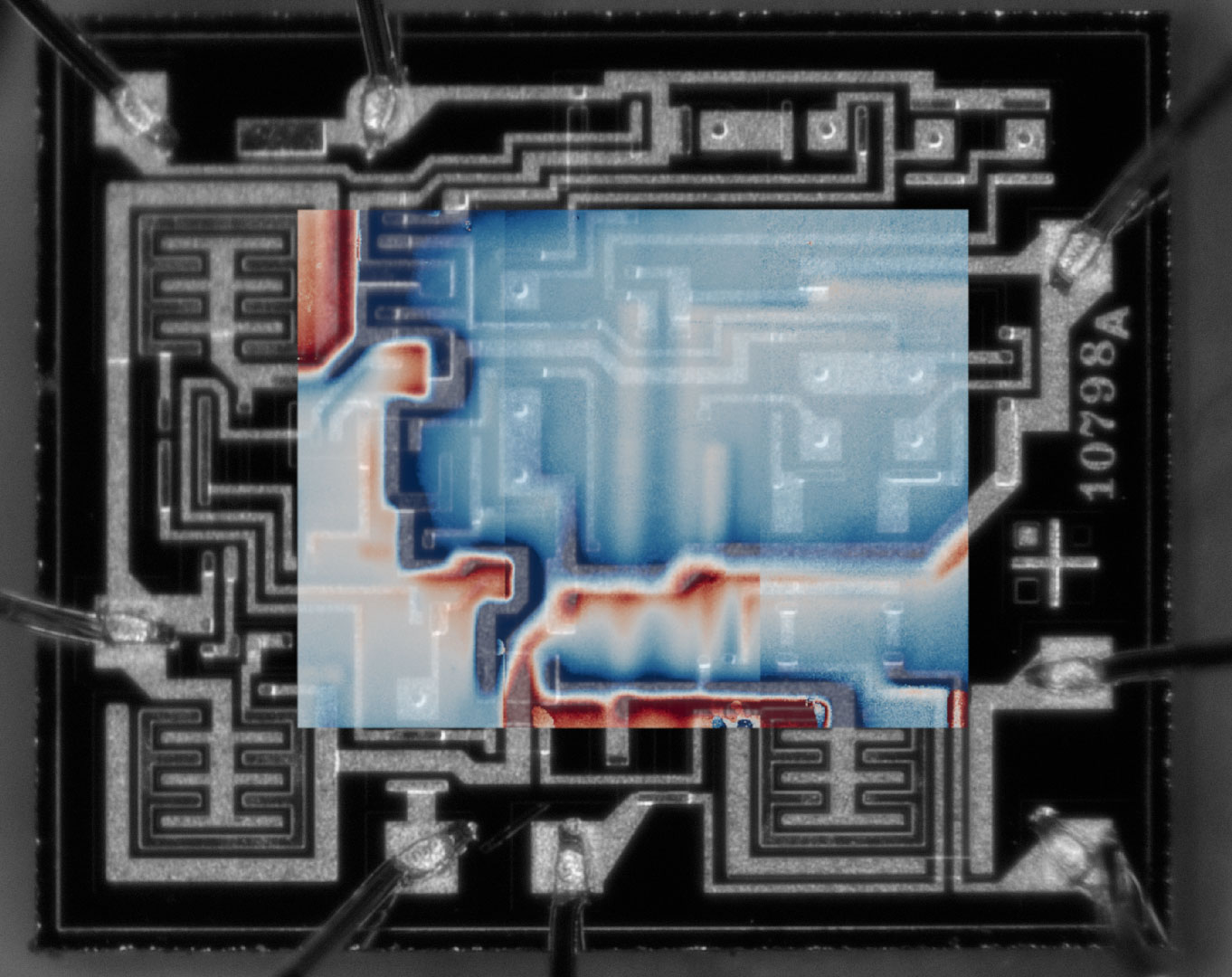
EuQlid’s Qu-MRI platform combines diamond-based quantum sensing, advanced signal processing, and machine learning to scan chips non-destructively and quickly uncover hidden defects, even on the production line. EuQlid’s innovation could “save chip foundries billions of dollars,” the company explained to Tom’s Hardware by way of an emailed press release.
Qu-MRI technology
EuQlid describes its new scanner as a device leveraging quantum magnetometry hardware to provide “buried electrical current maps with high-throughput and nano-amp sensitivity.”
The Qu-MRI relies on EuQlid’s first-gen product, the Quantum Diamond Microscope (QDM), augmented by advanced signal processing and AI-driven analytics to make sense of the complex semiconductor materials and devices this new product is targeting.

Potential impacts on industry
EuQlid’s new Qu-MRI offers compelling advantages over established chip-scanning tools. Rival methodologies may offer limited sub-surface imaging abilities, require physical contact with the chip, or deliver limited resolutions. Moreover, some investigation techniques require (time-consuming and destructive) grinding or slicing through chip layers for a full analysis.
Thus, contemporary destructive styles of chip inspection could be consigned to history by Qu-MRI. Moreover, EuQlid claims its solution is speedy and can enable earlier detection of buried defects during design validation, and it can even be deployed for inline production-time inspection for 3D ICs.

The new scanner could be an innovation that saves “billions.” Furthermore, the Qu-MRI targets a very healthy sector. The advanced metrology and inspection tools business exceeds $10 billion annually, says EuQlid, and is growing rapidly with the adoption of 3D architectures.
Get Tom's Hardware's best news and in-depth reviews, straight to your inbox.
According to Imec, the world’s leading R&D organization for semiconductor fabrication, “EuQlid’s Qu-MRI addresses a foundational technology need for the design and manufacturing of next-generation semiconductors, by non-invasively visualizing buried connectivity defects.”
Investors jump aboard already successful startup
EuQlid’s first-gen QDM is already in high demand for geoscience and bioimaging applications in prestigious academic institutions like Harvard University (USA), New York University (USA), Oxford University (UK), and Curtin University (Australia), among others. But, fueled by the new flagship semiconductor scanning solution, the Qu-MRI, significant new investments are now coming in.
Coinciding with the emergence of the Qu-MRI, EuQlid announced that it has just raised $3 million from lead investor QDNL Participations. Moreover, it has already secured over $1.5 million in early customer revenue. That’s a great start for the founding team, reaping the rewards from their expertise in atomic physics, quantum sensing, and the semiconductor industry.

Follow Tom's Hardware on Google News, or add us as a preferred source, to get our latest news, analysis, & reviews in your feeds.

Mark Tyson is a news editor at Tom's Hardware. He enjoys covering the full breadth of PC tech; from business and semiconductor design to products approaching the edge of reason.