Samsung's Taylor, Texas fab could herald a breakthrough for the chipmaker, company plans 2026 risk production — new production flows, pellicles for EUV patterning as site targets 50,000 WSPM
50,000 wafer starts per month?

Samsung Foundry is reportedly on track to hit the 'first light' milestone with ASML's EUV lithography systems at its Taylor Fab 1 in the coming month and commence risk production at the facility in the second half of the year, according to Hankyung. The new fab will not be Samsung's first fab with EUV scanners; however, it seems that the facility will be the company's largest logic fab when fully ramped. It will also be the first fab to adopt pellicles for EUV patterning, something that drastically changes production flows. Implementing pellicles and the sheer scale of the fab signal that it may well be a breakthrough facility for the company.
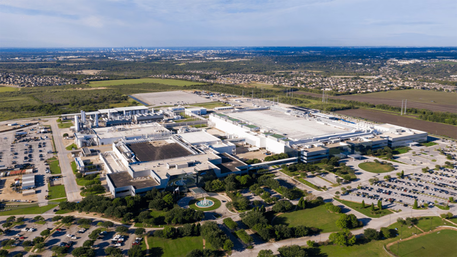
Samsung's biggest campus yet
When Samsung announced plans to build a new leading-edge semiconductor production facility near Taylor, Texas, the intention was to build a sophisticated fab that would cost $17 billion, with construction starting in 2022, and operations beginning in 2024.
Back then, the company only said that the new site would span more than 5 million square meters (1235 acres), which is larger than the company's domestic South Korea-based campuses near Pyeongtaek and Hwaseong. To put that number into context, Intel's Silicon Desert campus near Chandler, Arizona, which houses Fab 52 and Fab 62, is around 700 acres.
Samsung did not announce which nodes the new site would use initially, aside from mentioning that it would use advanced technologies to make chips for 5G, AI, HPC, and other demanding applications. Meanwhile, the whole project got bigger in April 2024, when Samsung disclosed plans to invest as much as $44 billion in the campus, building two advanced semiconductor fab modules, an advanced packaging facility, and an R&D center. In fact, given the area of the site, it is reasonable to expect Samsung to eventually build additional fab modules.

While the shell of the first fab module was completed in late 2024 – early 2025, the company delayed moving in expensive wafer fab equipment (WFE) because it was uncertain about the node strategy, volume demand, and the lack of a big-ticket customer. Following Tesla's announcements to use Samsung Foundry's Texas capacity to build AI6 chips through 2033 and AI5 chips before that, the questions surrounding a large customer and volume were answered. So, Samsung began to install advanced tools. The company is on track to reach the 'first light' milestone with ASML's EUV tools this March.
With the Tesla contracts signed, Samsung Foundry is now targeting 50,000 wafer starts per month (WSPM) of capacity using the SF2/SF3P process technology at the Taylor fab (according to TrendForce.) Though it is unclear whether this number only describes the first module, or the capacity of the whole $44 billion project that includes two fab modules.
In any case, 50,000 WSPM capacity is much higher compared to what Intel's Fab 52 can offer (40,000 WSPM), as well as higher than what TSMC's typical fab modules can process (around 20,000 WSPM). As a result, Samsung's Taylor fab will likely be the company's largest logic production site that the company has ever operated.
Possible Pellicle pilot
But in addition to being one of Samsung Foundry's largest fabs ever, the new facility will be the company's first fab to use pellicles for EUV lithography (according to Citrini analyst via @jukan05), something it has never done before, which will fundamentally change manufacturing flow at the fab.
Industry sources reportedly indicate that Samsung has ordered dedicated EUV pellicle attachment, detachment, and inspection systems for the Taylor fab. The contract, reportedly worth 25 billion won ($17.5 million), was awarded to FST, a Korean equipment supplier that has been developing pellicle handling solutions for several years.
These are production-grade systems designed to insert pellicles into a high-volume EUV flow. Readiness of these tools should confirm that Samsung intends to qualify pellicles for mass production rather than limited pilot use; however, this has not been officially confirmed by Samsung, and should therefore be taken with a grain of salt. The tools are said to support both conventional metal-silicide (MeSi) EUV pellicles and next-generation carbon nanotube pellicles, which gives Samsung an upgrade path.

For those not familiar, an EUV pellicle is an ultra-thin protective membrane mounted above a photomask during exposure to prevent particles from landing on the mask surface and printing defects onto the wafer. While pellicles have long been standard in deep ultraviolet lithography, EUV pellicles are far more difficult to make and use due to strict requirements for optical transmission, thermal durability, and mechanical stability under EUV radiation. For this reason, Samsung has so far avoided EUV pellicles because they were a net negative for its manufacturing economics and tool stability.
Early EUV pellicles transmitted only around 80% – 88% of 13.5-nm light, causing a 12–20% loss of photons at a time when ASML EUV sources had a performance of around 250W (early NXE:3400B/3400C machines), which would have cut wafer throughput and raised cost per wafer significantly due to longer exposures. At the same time, first-generation pellicles suffered from limited lifetime and thermal instability: they warped or even cracked as well as degraded under sustained EUV radiation, which increased downtime and pellicle failure risk.
Each pellicle can cost from tens of thousands to hundreds of thousands of dollars, so if its replacement cycle were short enough, it would inflate Samsung's costs to something that Samsung's margin structure could absorb. So instead of using pellicles, Samsung bet on a pellicle-free EUV flow based on ultra-clean mask handling, frequent reticle inspection and cleaning, and short mask reuse cycles, which preserved throughput and kept defect risk manageable for smaller dies and few EUV layers. However, the flip side of this decision is reportedly inconsistent yields and variability.
Now, ASML has delivered much more capable Twinscan NXE:3600D and NXE:3800E machines with much more powerful light sources and higher throughput. Also, the industry has introduced metal-silicide (and even carbon-nanotube pellicles, but Samsung will reportedly stick to MeSi pellicles) with better transmittance and durability, so using pellicles makes the most sense right now.
Furthermore, as Tesla's AI5 and other chips use SF2/SF3P and other advanced nodes use many more EUV layers than earlier EUV-based designs, the usage of pellicles becomes compulsory even for Samsung.
Pellicles sharply reduce stochastic mask-borne defects, which are increasingly dominant at the 2nm scale. For large logic dies (such as Tesla's AI5), a single particle on a critical EUV mask layer can destroy an entire chip or even repeat across multiple fields. By shifting the particle plane out of focus, pellicles dramatically lower this risk, thus improving yields and, more importantly, yield stability, something that Tesla clearly demands.
Fundamental shift for Samsung
Ultimately, Samsung will use its Taylor fab to make chips for other clients in addition to Tesla and perhaps introduction of pellicles to the flow will greatly improve the company's positions on the foundry market as inconsistent wafer-to-wafer and lot-to-lot yields and performance variability is what has historically plagued Samsung Foundry's EUV-based nodes and prevented their usage by clients with larger dies.

Anton Shilov is a contributing writer at Tom’s Hardware. Over the past couple of decades, he has covered everything from CPUs and GPUs to supercomputers and from modern process technologies and latest fab tools to high-tech industry trends.
