 Join Tom’s Hardware today


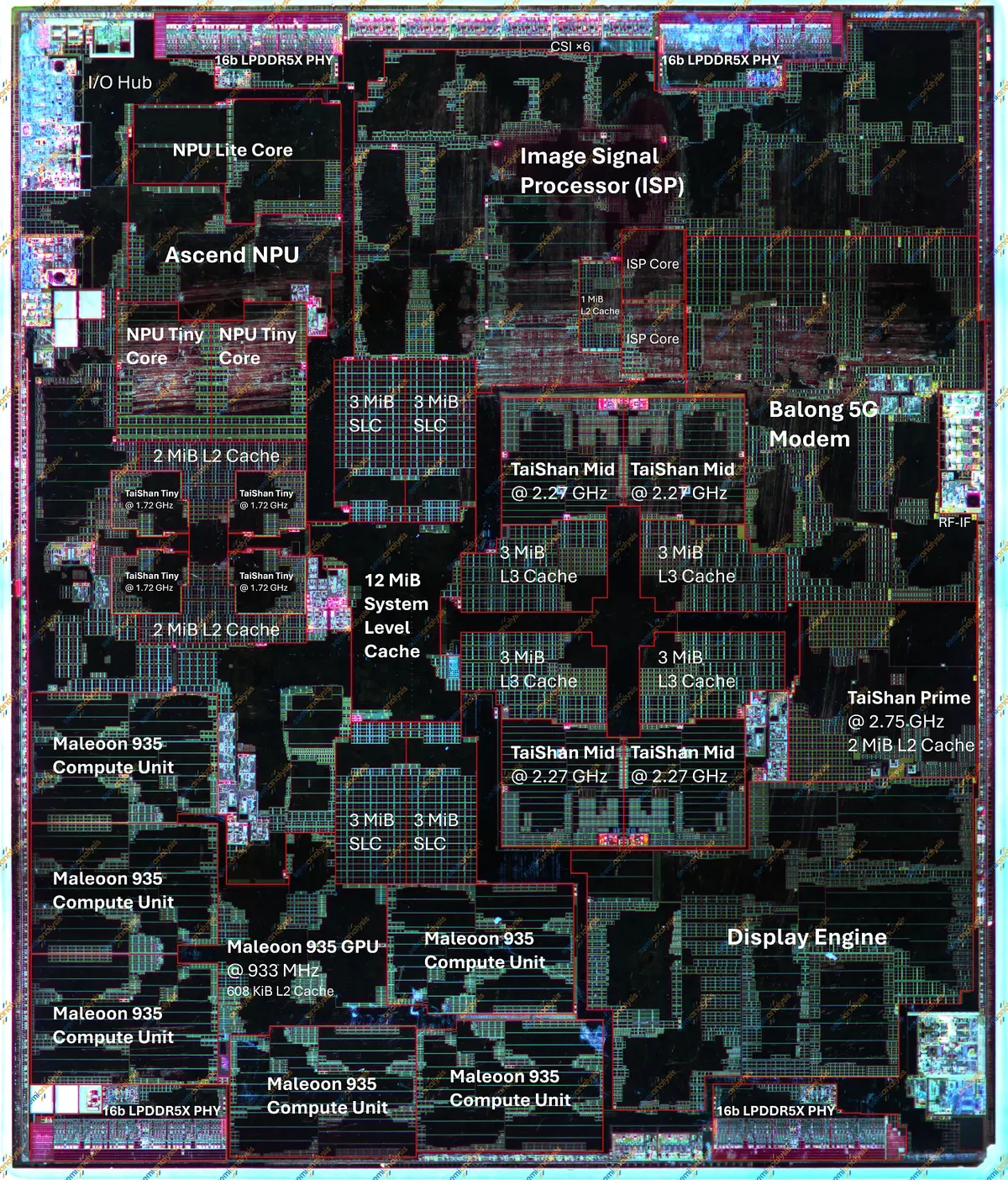
SemiAnalysis has published the first teardown from its new in-house lab, focusing on the minimum local metal pitch on SMIC’s third-gen 7nm at 32.5nm, tighter than the 36nm pitch shipping in Intel’s Panther Lake chips on 18A. The analysis was conducted on a HiSilicon Kirin 9030, the processor found inside Huawei’s Mate 80 phones and built on the N+3 process, which SemiAnalysis says trails Intel’s 18A high-density library by 38%. The SemiAnalysis Teardown Engineering & Evaluation Lab (STEEL) has been opened in Hillsboro, Oregon, and built to take on TechInsights in advanced-node reverse engineering.
A 36nm pitch is what Panther Lake ships with, but the 18A process on the whole supports a 32nm minimum metal pitch. With Panter Lake, Intel opted to relax the pitch because routing power through the back of the wafer — via PowerVia — clears the front-side metal stack for signal wiring.
Intel has said doing this buys roughly 10% higher density and looser front-side pitches, which is how a node built on GAA RibbonFET transistors and backside power can ship a wider local pitch than a DUV Chinese process and maintain a wide overall lead. SMIC reached 32.5nm without EUV lithography, leaning on DUV tools and quadruple-patterning that needs extra masking and etch passes.
Counting transistors per area, SemiAnalysis put N+3 at 113.4 million per square millimeter, just ahead of TSMC's mature N6 at 107.7 million and well behind 18A. SMIC got there by spending every density trick available without EUV: two fins per transistor, contacts landed directly over the active gate, and single diffusion breaks between cells.
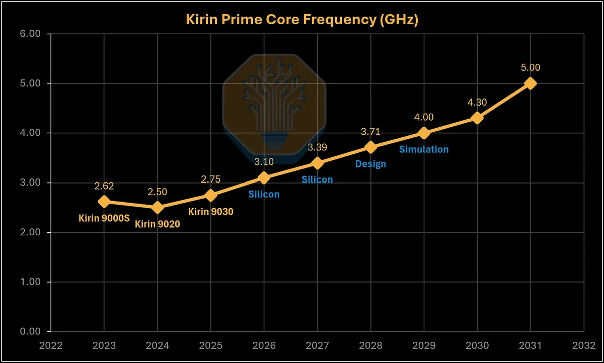
Each of those workarounds obviously adds complexity and cost, with N+3’s ceiling ultimately showing a huge trade-off. The Kirin 9030 Pro's prime core runs at 2.75 GHz and lands near Arm's 2021-era Cortex-X2 per clock, leaving the chip roughly level with Android flagships from three years ago and behind current parts from Apple, Qualcomm, MediaTek, and Samsung. Huawei’s roadmap does say that it’s targeting 5 GHz by 2031, but, as SemiAnalysis notes, that’s “far beyond what planar scaling alone could deliver.”
SemiAnalysis said it spent the past 18 months building the lab and has already earned revenue analyzing datacenter silicon. “We have already generated revenue on advanced datacenter chip teardowns, including our recent reverse engineering of a major TSMC customer’s COUPE CPO optical engine + EIC 3D stack.”
The company is taking aim at the Ottawa-based TechInsights, which is backed by private equity and held by the likes of Oakley Capital and CVC Growth. SemiAnalysis claims its rival is up for sale and has underinvested in equipment as a result, though that hasn’t been officially confirmed. The teardown also found the Kirin 9030 Pro carrying Samsung LPDDR5X memory, with 16 GB variants turning up DRAM from Chinese maker CXMT as well.

Follow Tom's Hardware on Google News, or add us as a preferred source, to get our latest news, analysis, & reviews in your feeds.
