Tokyo Electron's new tool can reduce the necessity for EUV double patterning and improve yield
Is there no need for High-NA for now?

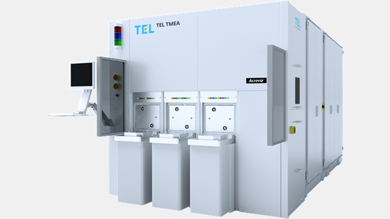
Tokyo Electron has introduced its Acrevia, a new gas cluster beam (GCB) system tailored for refining patterns created by EUV lithography. The tool, which uses low-damage surface processing, can be used for several things, including reducing the usage of EUV multi-patterning for upcoming nodes, enhancing line edge roughness to reduce performance variability, reducing stochastic litho defects, and ultimately cutting chipmaking costs and improving yields.
Modern EUV lithography tools with 0.33 numerical aperture optics (Low-NA EUV) can achieve critical dimensions of 13 nm to 16 nm for high-volume production with a single exposure. Printing a 26-nm minimum metal pitch is enough, acceptable for 3nm-class process technologies. To print finer circuits with smaller metal pitches for 2nm-class production nodes and beyond, chipmakers have to either use an EUV lithography machine with a 0.55 numerical aperture optics (High-NA EUV), Low-NA EUV double patterning, Applied Materials’s Centura Sculpta pattern shaping tool, or, now Tokyo Electron’s Acrevia.
A standard single EUV patterning process flow consists of eight key steps: wafer deposition, chemical-mechanical polishing clean, lithography, metrology, pattern etch, clean, metrology, and wafer etch. All the steps (except the wafer etch) are repeated for double patterning.
Article continues belowHowever, the double patterning EUV technique introduces new challenges, including increased costs, potentially lower yields, and an extended production cycle. Instead of double patterning, Tokyo Electron proposes inserting its Acrevia tool into the process technology flow after lithography patterning and subsequent dry etching steps. It can also be used after double or even triple EUV patterning to refine it if needed.
The directional gas cluster beam irradiates the patterned features, etching the feature sidewalls at an optimal wafer tilting angle to adjust critical dimensions and refine patterns, which will prevent the usage of EUV double patterning in some cases. Acrevia’s precise wafer scanning system — based on the Location Specific Processing (LSP) technology — can control the etching amount at any point, ensuring exceptional within-wafer uniformity correction.
EUV lithography is known for stochastic effects arising from the low photon-absorption density in EUV resists. These effects lead to random bridge defects and poor line-edge roughness, among other issues. Due to their random nature, these defects are difficult to detect. Even with EUV double patterning (which essentially allows the relaxation of critical dimensions of each pattern), they cannot be entirely eradicated. Tokyo Electron says that its pattern-refinement tool can improve line edge roughness (LER) on pattern sidewalls and decrease stochastic litho defects, thereby improving yield.
While the Acrevia tool will not replace double or triple EUV patterning, it could reduce its usage and refine patterns, improving performance and yield, which is a big deal.
Get Tom's Hardware's best news and in-depth reviews, straight to your inbox.
“Acrevia features our original technology that enables high etch rate and low damage patterning,” says Hiroshi Ishida, General Manager, DSS BU at Tokyo Electron. “In the increasingly challenging field of advanced patterning, Acrevia makes further scaling possible and maximizes productivity. Going forward, we will keep developing technologies that exceed customers’ expectations and contribute to the advancement of semiconductor devices.”

Anton Shilov is a contributing writer at Tom’s Hardware. Over the past couple of decades, he has covered everything from CPUs and GPUs to supercomputers and from modern process technologies and latest fab tools to high-tech industry trends.
-
edzieba Whilst it sounds attractive, how many will really bet on spending a few hundred million dollars on a new machine and adding a new process step (or rather, steps, as it will still need clean and metrology steps added to bracket this new etch step), rather than running wafers through their existing machines as a repeated process step?Reply