TSMC to build massive chips twice the size of today's largest — chips will use thousands of watts of power
120x120mm chips with 12 HBM4E stacks in 2027

Thought AMD's Instinct MI300X and Nvidia's B200 GPUs were huge? Think again: TSMC is working on a version of its chip-on-wafer-on-substrate (CoWoS) packaging technology that will enable system-in-packages (SiPs) over two times bigger, the company announced at its North American Technology Symposium. These will use 120x120mm monstrous packages and will draw kilowatts of power, the foundry envisions.
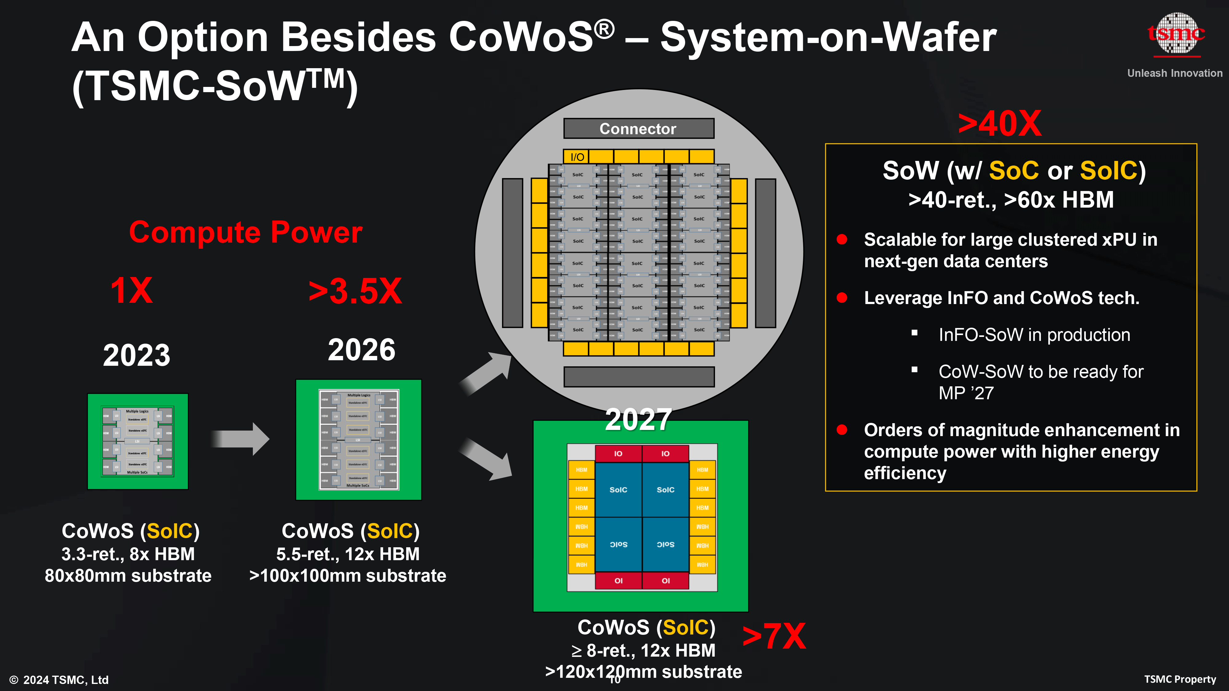
The latest version of CoWoS allows TSMC to build silicon interposers that are about 3.3 times larger than the size of a photomask (or reticle, which is 858mm2). Thus, logic, eight HBM3/HBM3E memory stacks, I/O, and other chiplets can occupy up to 2831 mm2. The maximum substrate size is 80×80 mm. AMD's Instinct MI300X and Nvidia's B200 use this technology, though Nvidia's B200 processor is bigger than AMD's MI300X.
The next generation CoWoS_L, due to be ready for production in 2026, will be capable of enabling interposers of around 5.5 times the reticle size (which may not be as impressive as the 6x reticle size announced last year). This means 4719 mm2 will be available for logic, up to 12 HBM memory stacks, and other chiplets. Such SiPs will also require larger substrates, and based on TSMC's slide, we are looking at 100x100 mm. As a result, such processors will not be able to use OAM modules.
TSMC won't stop there: In 2027, it will have a version of CoWoS technology that will enable interposers eight or more times the reticle size, which will give chiplets 6,864 square mm of space. One of the designs that TSMC envisions relies on four stacked systems-on-integrated chips (SoICs) mated with 12 HBM4 memory stacks and additional I/O dies. Such a giant will certainly draw an enormous amount of power — we are talking about thousands of watts here and will need a very sophisticated cooling technology. TSMC also expects such solutions to use a 120x120mm substrate.
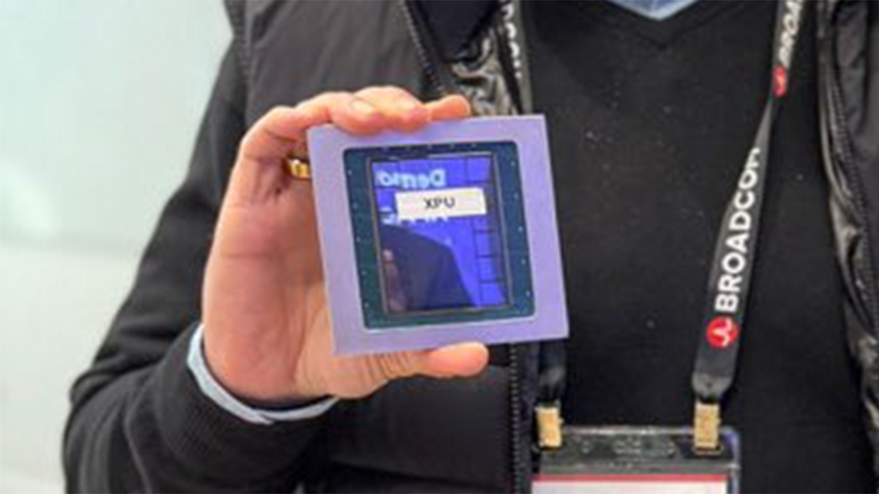
Interestingly, earlier this year, Broadcom demonstrated a custom-built AI processor featuring two logic dies and 12 HBM memory stacks. We do not have specifications for this one, but it looks bigger than AMD's Instinct MI300X and Nvidia's B200, though not as big as what TSMC plans for 2027.
Get Tom's Hardware's best news and in-depth reviews, straight to your inbox.

Anton Shilov is a contributing writer at Tom’s Hardware. Over the past couple of decades, he has covered everything from CPUs and GPUs to supercomputers and from modern process technologies and latest fab tools to high-tech industry trends.
-
Alvar "Miles" Udell ReplyTSMC to build massive chips twice the size of today's largest — chips will use thousands of watts of power
So it's going to be twice as large as the Cerebras Wafer Scale Engine 3?
-
Pierce2623 Reply
Ehh the Cerebras is a pipe dream that they can’t get working right at a decent price. They still haven’t even managed to get samples out.Alvar Miles Udell said:So it's going to be twice as large as the Cerebras Wafer Scale Engine 3?
-
endocine Reply
They exported some to ChinaPierce2623 said:Ehh the Cerebras is a pipe dream that they can’t get working right at a decent price. They still haven’t even managed to get samples out. -
subspruce Reply
no a chip like that will be super expensive and only for the enterprise marketrazor512 said:Any chance those chips will make their way down to the consumer/ home user level? -
CmdrShepard Reply
Yeah, you will just need $10m to buy one and a nuclear power plant to power it. Piece of cake, as a matter of fact I've already ordered ten of those. /srazor512 said:Any chance those chips will make their way down to the consumer/ home user level? -
TJ Hooker Reply
There are multiple customers claiming to be using Cerebras' chips as early as 2020. How would this be possible if they can't even get working samples out?Pierce2623 said:Ehh the Cerebras is a pipe dream that they can’t get working right at a decent price. They still haven’t even managed to get samples out.
https://www.hpcwire.com/2020/10/13/llnl-anl-and-gsk-provide-early-glimpse-into-cerebras-ai-system-performance/
https://www.zdnet.com/article/glaxos-biology-research-with-novel-cerebras-machine-shows-hardware-may-change-how-ai-is-done/ -
RyderXx Reply
yea lol, i think Cerebras WSE-3 is still going to be better than TSMC. the WSE-3 is 4 trillion transistorAlvar Miles Udell said:So it's going to be twice as large as the Cerebras Wafer Scale Engine 3?
-
TheOtherOne In the future, we might actually end up with the old age prediction coming true about the size computers bigger than rooms and I forgot the rest but I think it was also predicted that it will require all the water from Niagara Falls to cool it down or something.. :homer:Reply -
subspruce Reply
That niagara falls joke might get real with how much Intel is pushing their CPUs and how much Nvidia is pushing their GPUs.TheOtherOne said:In the future, we might actually end up with the old age prediction coming true about the size computers bigger than rooms and I forgot the rest but I think it was also predicted that it will require all the water from Niagara Falls to cool it down or something.. :homer:
