TSMC's second 2nm fab could be ready earlier than expected — the company could deploy two leading-edge fabs at once
But who will use all that capacity?

Get Tom's Hardware's best news and in-depth reviews, straight to your inbox.
You are now subscribed
Your newsletter sign-up was successful
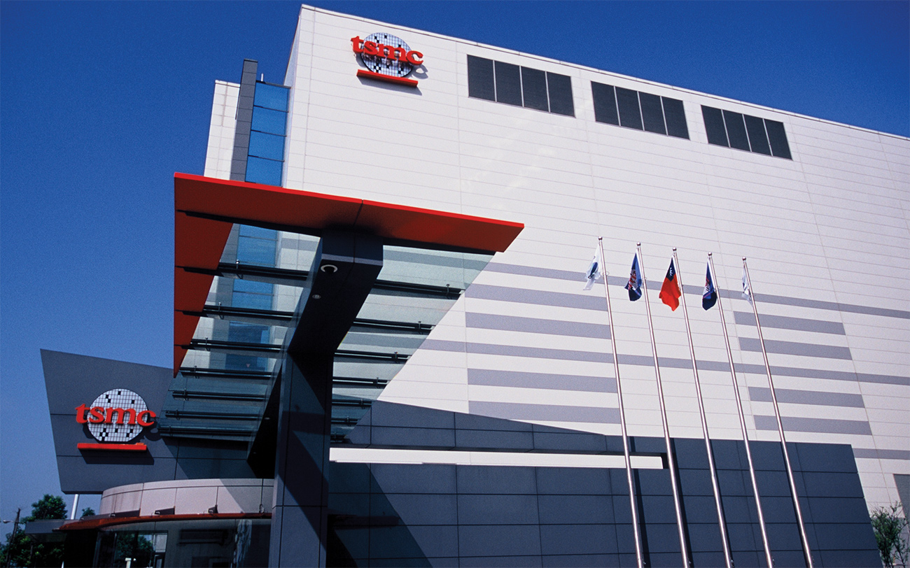
TSMC's second fab capable of processing wafers using the company's N2 process technology (2nm-class) could be ready in Kaohsiung Science Park somewhat ahead of schedule, reports China Times. However, this news should be taken with a grain of salt, as it hasn't been confirmed by TSMC. Also, the foundry has reportedly obtained all the necessary permissions to construct another fab in Kaohsiung Science Park.
The report from China Times also claims that phase 1 of TSMC's N2-capable fab near Kaohsiung aims to start mass production in 2025, which is a bit earlier than expected as typically the company does not deploy two leading-edge fabs at once.
TSMC is prepping to build at least two N2-capable fabs in Taiwan. The first fabrication facility is set to be situated near Baoshan in Hsinchu County, adjacent to its R1 research and development center, which is focused on N2 technology development. As planned, this fab is set to start high-volume manufacturing (HVM) of 2nm chips in the second half of 2025. TSMC's second N2-capable fab is set to be located in the Kaohsiung Science Park, a segment of the Southern Taiwan Science Park near Kaohsiung. This fab is meant to start HVM a bit later, presumably in 2026.
Although TSMC's N2-capable fab phase 1 in Kaohsiung Science Park could be ready ahead of schedule, there are two big questions; First, will TSMC invest in equipping it ahead of schedule, given that the company has been cautious with CapEx increases in recent quarters? Second, even if it installs all the necessary tools into this fab, will it have enough clients to use that capacity, given that 2nm process technologies are expected to be extremely expensive for fabless customers?
There could be one reason for TSMC to enable as much 2nm capacity as possible in 2025: intensified competition from Intel and Samsung Foundry and the desire to ensure that it can serve all the clients willing to pay a premium for the latest process technologies and require huge volumes. Meanwhile, there are not many such companies these days.
While we should probably consider information about TSMC's N2-capable fab phase 1 in Kaohsiung Science Park, the report also says that phase 2 of the facility has received all the necessary permissions and licenses, which is why TSMC will be able to start prepping for building the fab early in 2024.
Get Tom's Hardware's best news and in-depth reviews, straight to your inbox.

Anton Shilov is a contributing writer at Tom’s Hardware. Over the past couple of decades, he has covered everything from CPUs and GPUs to supercomputers and from modern process technologies and latest fab tools to high-tech industry trends.
-
phead128 ReplyHowever, this news should be taken with a grain of salt, as it hasn't been confirmed by TSMC.
So the true nature of journalism today.... catchy titles/headlines, then the reality is... it's false. Then don't waste our time publishing! -
jaquith If I were a Taiwanese company I would be diversifying outside of Taiwan. When China finally gets enough gusto to reclaim Taiwan, it's going to bring the chip market to a dangerously low volume like what we saw during COVID-19 or worse where companies literally are stopped in their production tracks unable to complete items for sale.Reply
Just know the second that China invades Taiwan, the United States will make a crater out of TSMC fabrication and similar critical facilities.