Tesla Packs 50 Billion Transistors Onto D1 Dojo Chip Designed to Conquer Artificial Intelligence Training
D1 deliver 362 TeraFLOPs of power
Get Tom's Hardware's best news and in-depth reviews, straight to your inbox.
You are now subscribed
Your newsletter sign-up was successful
Artificial intelligence (AI) has seen a broad adoption over the past couple of years. At Tesla, who as many know is a company that works on electric and autonomous vehicles, AI has a massive value to every aspect of the company's work. To speed up the AI software workloads, Tesla has today presented its D1 Dojo custom application-specific integrated circuit (ASIC) for AI training.
There are currently many companies building ASICs for AI workloads. Everyone from countless number of start-ups, all the way to big players like Amazon, Baidu, Intel and NVIDIA. However, not everyone gets the formula right and not everyone can satisfy each workload perfectly. That is the reason why Tesla opted to develop its own ASIC for AI training purposes.
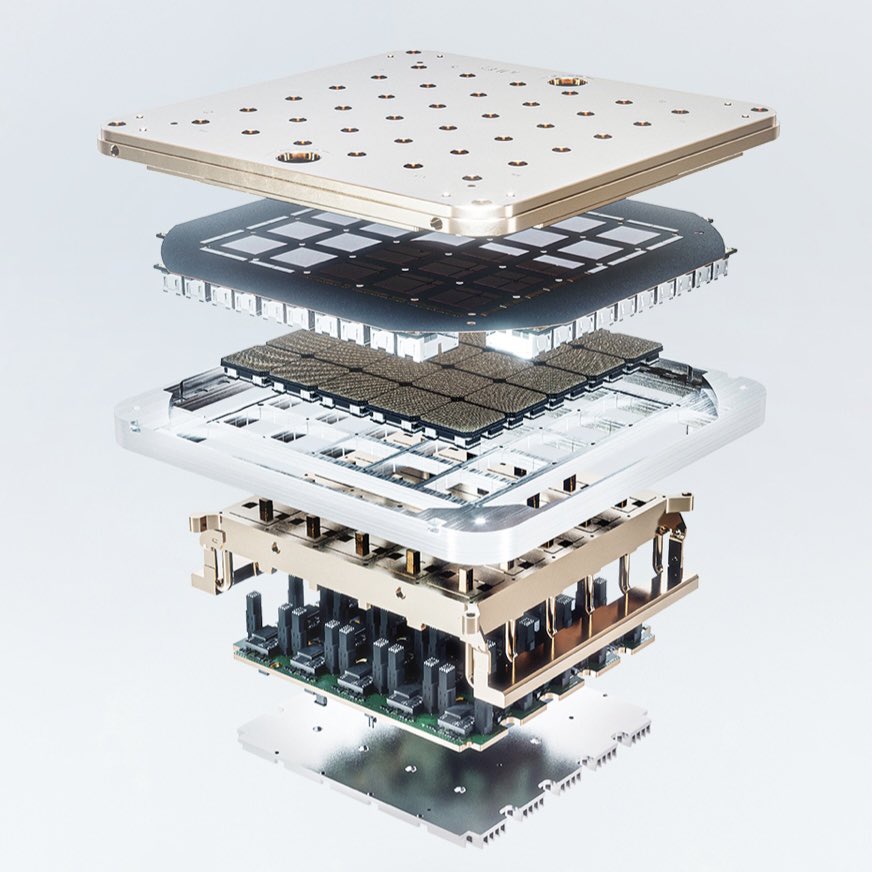
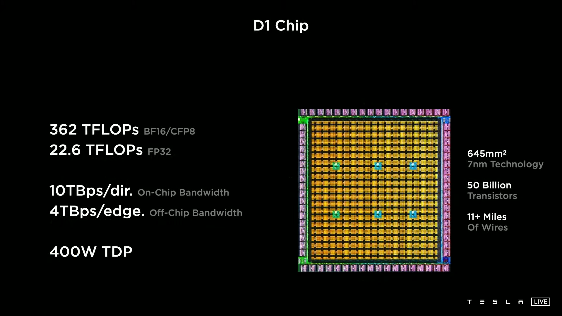
Called the D1, the chip resembles a part of the Dojo supercomputer used to train AI models inside Tesla HQ, which are later deployed in various applications. The D1 chip is a product of TSMC's manufacturing efforts, forged in a 7nm semiconductor node. Packing over 50 billion transistors, the chip boasts a huge die size of 645mm^2.
Article continues belowThe chip has some impressive performance claims, where Tesla states that it can output as much as 362 TeraFLOPs at FP16/CFP8 precision or about 22.6 TeraFLOPs of single-precision FP32 tasks. It is clear that Tesla optimized for FP16 data types, where they have managed to beat even the current leader in compute power - Nvidia. Nvidia's A100 Ampere GPU is capable of producing "only" 312 TeraFLOPs of power at FP16 workloads — and with sparsity, it can do up to double that.
Going to the silicon level, we see that Tesla built a mesh of functional units (FUs) that are interconnected together to form one massive chip. Each FU contains a 64-bit CPU with custom ISA, designed for transposes, gathers, broadcasts, and link traversals. The CPU design itself is a superscalar implementation with a 4-wide scalar and 2-wide vector pipelines. Looking at the images below, you can see that the FU is built with a big block for single instruction multiple data (SIMD) floating-point and integer processing elements. Each FU has its own 1.25MB scratchpad SRAM memory.
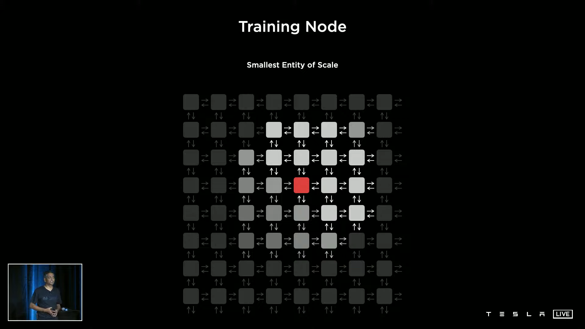
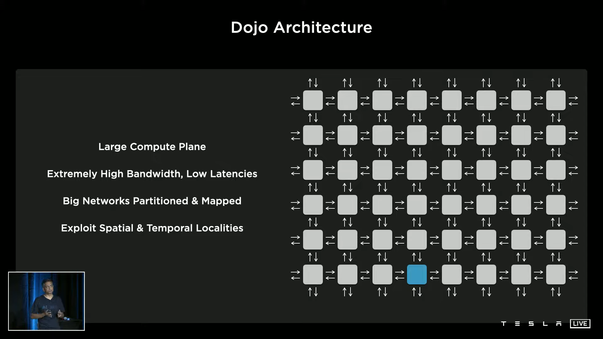
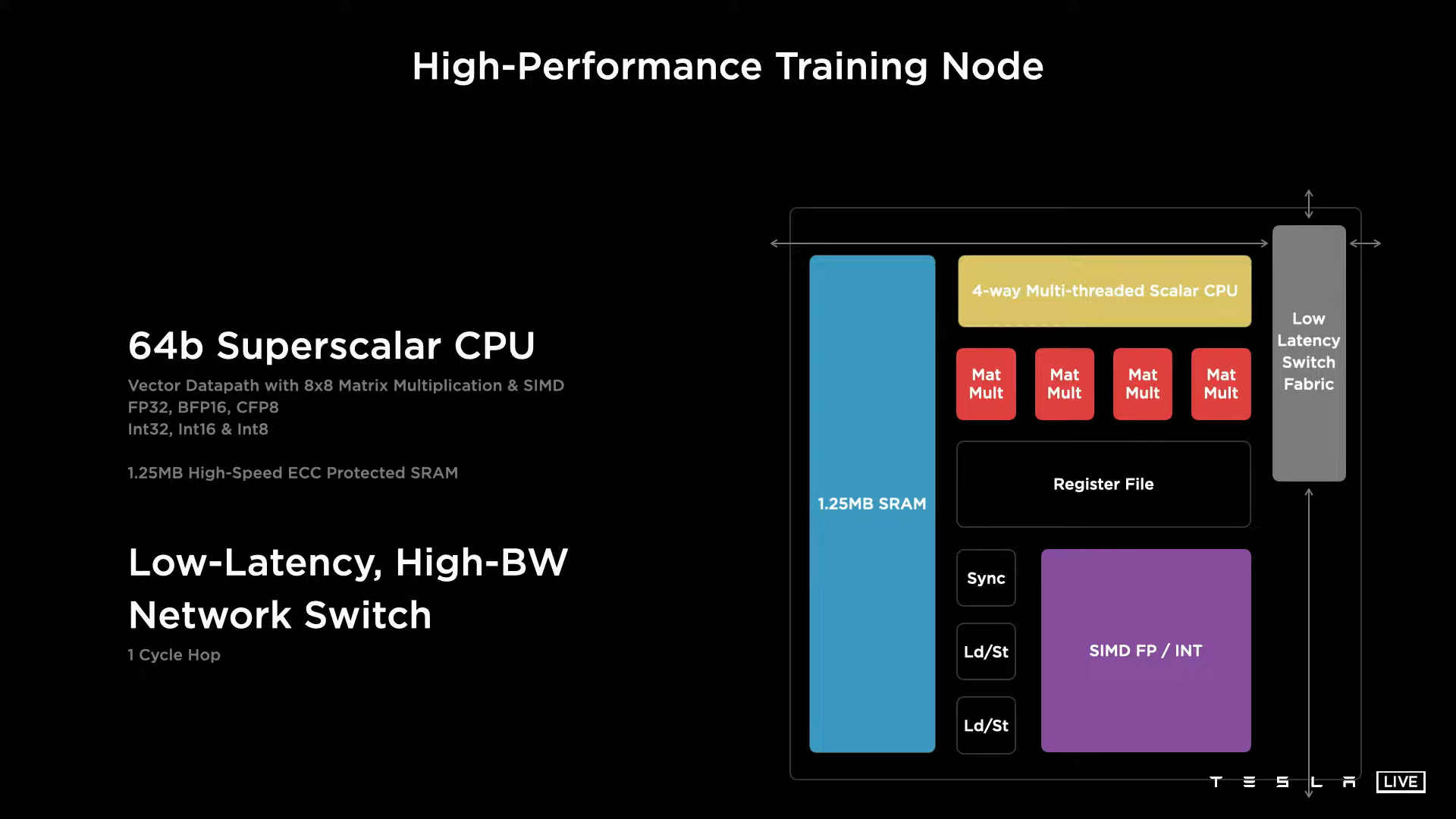
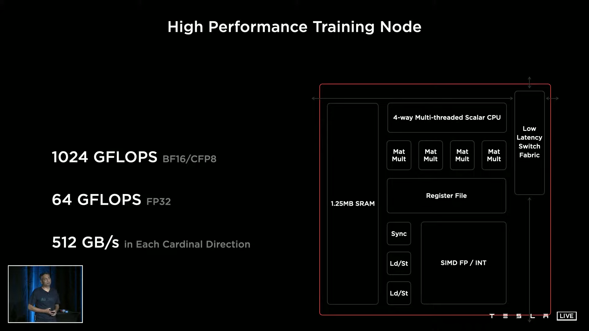
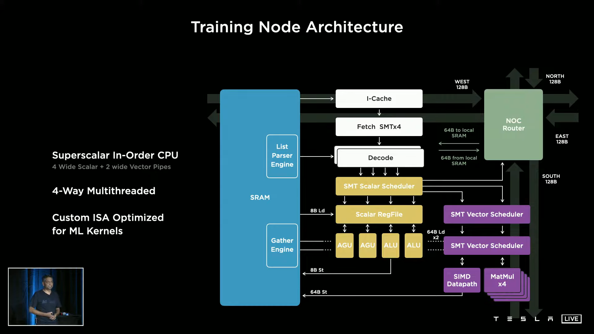
The FU itself is capable of performing one TeraFLOP of BF16 or CFP8, 64 GigaFLOPs of FP32 computation, and has 512 GB/s bandwidth in any direction in the mesh. The mesh is designed to traverse the FUs in only a single clock cycle, meaning that latencies are reduced and performance is increased. For more details, you can watch the Tesla AI day replay here.
Get Tom's Hardware's best news and in-depth reviews, straight to your inbox.
-
pjmelect I wonder how good they are it mining and if Elon is using them to increase his bit coin collection?Reply